Light-emitting diode with passivation layer and preparation method thereof

A technology for light-emitting diodes and a manufacturing method, which is applied to electrical components, circuits, semiconductor devices, etc., can solve the problems of no obvious improvement in luminous efficiency, poor effect of auxiliary current diffusion, and poor thickness and width design, so as to achieve good diffusion current. Effect, uniform luminescence, the effect of improving luminous efficiency

Inactive Publication Date: 2011-01-12
UBILUX OPTOELECTRONICS CORP
View PDF0 Cites 9 Cited by
  • Summary
  • Abstract
  • Description
  • Claims
  • Application Information

AI Technical Summary

Problems solved by technology

However, previous studies have not considered the width and thickness of the passivation layer 14, often resulting in that even if the passivation layer 14 is provided, the effect of assisting current diffusion is not good due to poor design of the thickness and width, and the luminous efficiency is not good. Significantly improved

Method used


Image

  • Light-emitting diode with passivation layer and preparation method thereof
  • Light-emitting diode with passivation layer and preparation method thereof
  • Light-emitting diode with passivation layer and preparation method thereof

Examples


Embodiment Construction

[0039] The present invention will be described in detail below with reference to the accompanying drawings and embodiments. It should be noted that in the following description, similar elements are denoted by the same numerals.

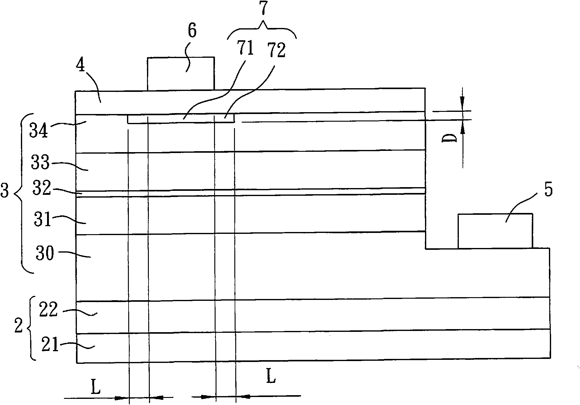
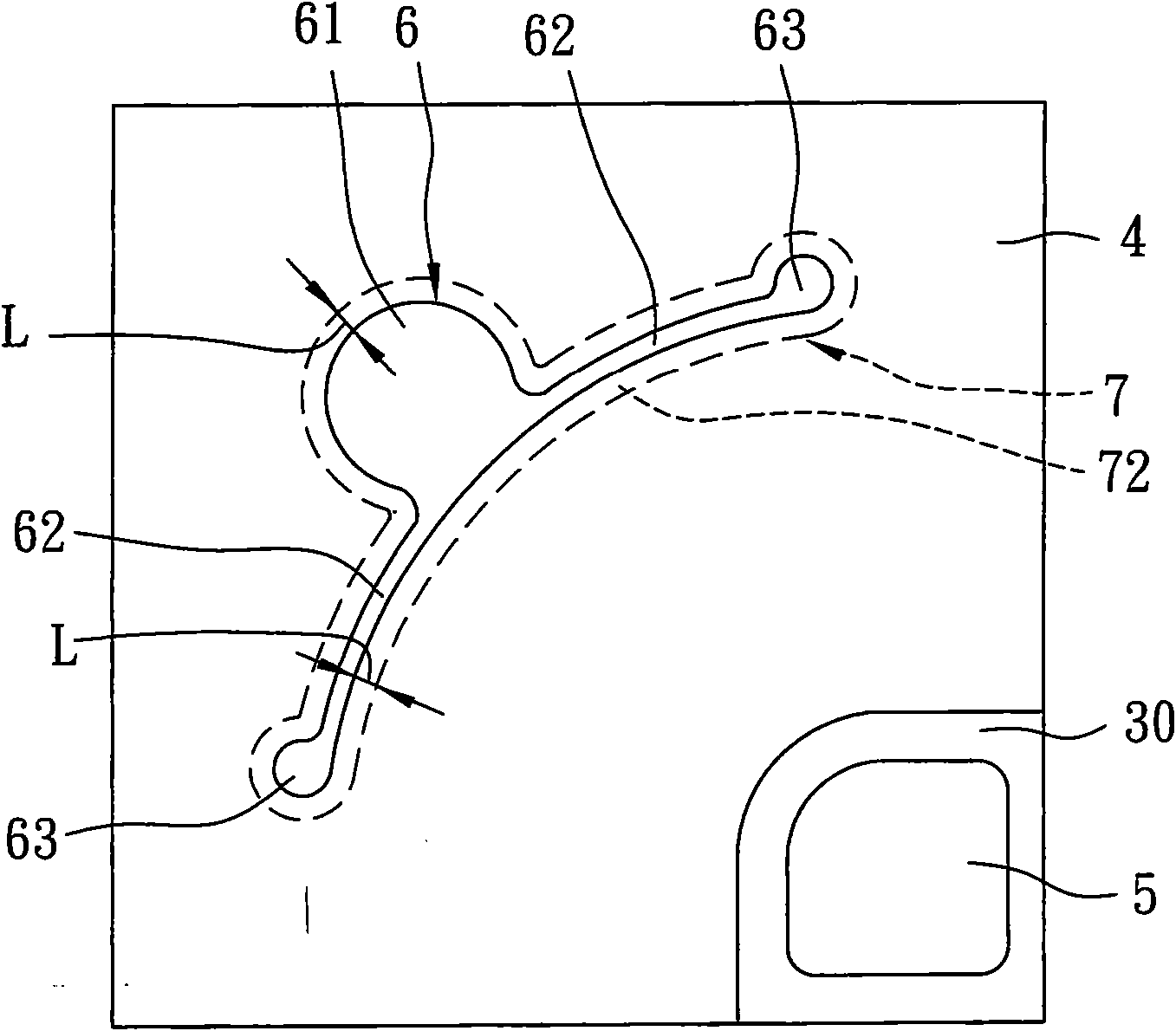
[0040] refer to figure 2 , image 3 , the first preferred embodiment of the light-emitting diode with a passivation layer in the present invention includes: a substrate 2, a light-emitting unit 3, a transparent conductive layer 4, a first electrode 5 electrically connected to the light-emitting unit 3, and a The second electrode 6 and a passivation layer 7 .

[0041] The base material 2 includes a substrate 21 and a buffer layer 22 coated on the surface of the substrate 21 . The substrate 21 of this embodiment is a sapphire substrate 21 , and the buffer layer 22 is made of undoped gallium nitride (GaN) material.

[0042] The light-emitting unit 3 is coated on the surface of the buffer layer 22 of the substrate 2, and along the direction from adja...


PUM

PropertyMeasurementUnit
widthaaaaaaaaaa

Abstract

The invention provides a light-emitting diode with a passivation layer and a preparation method thereof. The light-emitting diode comprises a base material, a light-emitting unit arranged on the base material, a first electrode, a second electrode and the passivation layer. The main improvement of the invention is that the passivation layer is arranged on the light-emitting unit and is positioned below the second electrode correspondingly; the passivation layer comprises a body part corresponding to the second electrode and an extension part connected at the periphery of the body part; the width of the extension part is L, wherein, L is more than or equal to 3 microns and is less than or equal to 20 microns; and the thickness of the passivation layer is D, wherein, D is more than or equal to 4 angstroms. The light-emitting diode of the invention is designed according to the appropriate width of the extension part and the thickness of the passivation layer, has good current diffusion effect, and achieves the purposes of the light-emitting uniformity and the promoted light-emitting efficiency.

Description

technical field [0001] The invention relates to a light-emitting diode and its manufacturing method, in particular to a light-emitting diode with a passivation layer and its manufacturing method which utilizes a surface treatment method to form a passivation layer to improve the uniformity of current distribution and luminous efficiency. Background technique [0002] refer to figure 1 , the conventional light emitting diode 1 includes: a substrate 11, a buffer layer 12 coated on the surface of the substrate 11, a light emitting unit 13, a passivation layer 14, a transparent conductive layer 15, an n-side electrode 16 and a p side electrodes 17 . The light emitting unit 13 sequentially includes: an n-type contact layer 131 , an n-type cladding layer 132 , a light-emitting layer 133 , a p-type cladding layer 134 and a p-type contact layer 135 from bottom to top. The n-side electrode 16 is arranged on the exposed surface of the n-type contact layer 131, and the p-side electro...

Claims


Application Information

Patent Timeline
Patent Type & Authority Applications(China)
IPC IPC(8): H01L33/00
Inventor 林志胜吴哲雄
Owner UBILUX OPTOELECTRONICS CORP
Why Eureka
Try Eureka