Insulating layer, printed circuit board with electronic component and producing method thereof

A technology for printed circuit boards and electronic components, which is applied in the directions of printed circuits connected with non-printed electrical components, assembling printed circuits with electrical components, and printed circuit components, etc., and can solve problems such as deformation of electronic components

Inactive Publication Date: 2011-01-19
SAMSUNG ELECTRO MECHANICS CO LTD
View PDF5 Cites 9 Cited by
  • Summary
  • Abstract
  • Description
  • Claims
  • Application Information

AI Technical Summary

Problems solved by technology

[0008] The present invention provides an insulating substrate, a printed circuit board embedded with electronic components, and a method of manufacturing the printed circuit board even in the case where a lay-up process is performed by using a thin insulating layer ...

Method used


Image

  • Insulating layer, printed circuit board with electronic component and producing method thereof
  • Insulating layer, printed circuit board with electronic component and producing method thereof
  • Insulating layer, printed circuit board with electronic component and producing method thereof

Examples


Embodiment Construction

[0021] Since there are variations and many embodiments of the invention, specific embodiments will be shown in the drawings and described in detail in the specification. However, this is not intended to limit the present invention to specific embodiments, and it should be understood that all changes, equivalents and substitutions are included in the present invention without departing from the spirit and technical scope of the present invention .

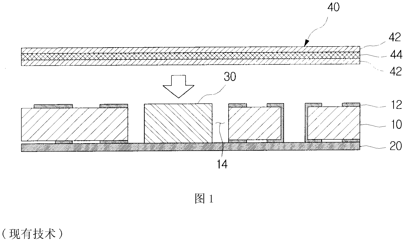
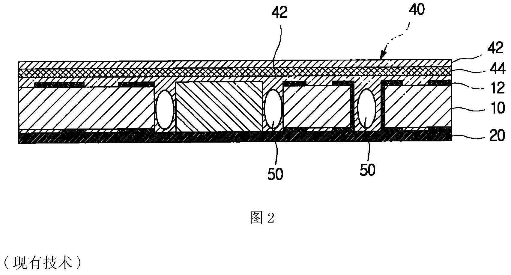
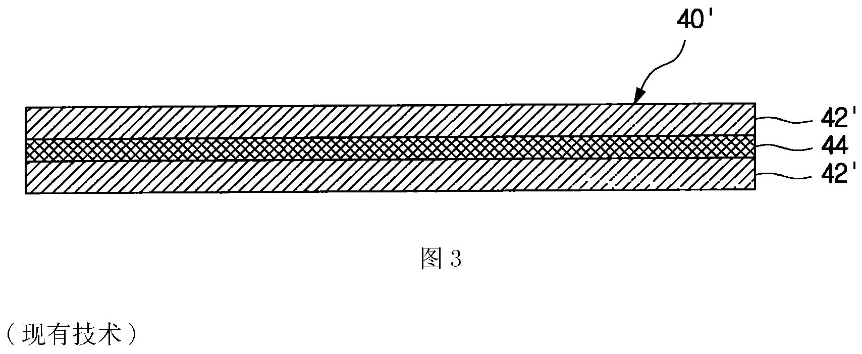
[0022] A method of manufacturing a printed circuit board embedded with electronic components according to some embodiments of the present invention will be described in more detail below with reference to the accompanying drawings. Those same or corresponding components are given the same reference numerals regardless of the figure number, and repeated descriptions are omitted.

[0023] Figure 5 is a flowchart illustrating a method of manufacturing a printed circuit board embedded with electronic components according to one embod...


PUM


Abstract

The invention discloses a printed circuit board with electronic component and producing method thereof. The method comprises steps of providing the circuit pattern chip plate which is disposed on the surface and is penetrated by a hollow cavity; bonding an adhesion layer to the lower surface of the chip plate to cover the hollow cavity; disposing an electronic component on the upper surface of the adhesion layer, corresponding to the position of the hollow cavity; stacking a first insulating layer which dose not have supporting materials filled in the hollow cavity on the upper surface of thechip plate to cover the circuit pattern so that the hollow cavity is filled; stacking a second insulating layer which has supporting materials filled in the hollow cavity on the upper side and the lower side of the chip plate.

Description

[0001] References to related applications [0002] This application claims the priority of Korean Patent Application No. 10-2009-0062095 and No. 10-2009-0114119 filed with the Korean Intellectual Property Office on July 8, 2009 and November 24, 2009, respectively, the disclosure of which is in its entirety The contents are hereby incorporated by reference. technical field [0003] The invention relates to an insulating layer, a printed circuit board embedded with electronic components and a manufacturing method of the printed circuit board. Background technique [0004] With the development of the electronics industry, there is an increasing demand for smaller and more functional electronic components. Specifically, market trends based on lighter, thinner, shorter and smaller personal mobile devices have resulted in thinner printed circuit boards. As a result, component mounting methods different from conventional methods have emerged. An example is an embedded printed ci...

Claims


Application Information

Patent Timeline
IPC IPC(8): H05K3/30H05K1/18H05K1/02
Inventor 李相澈郑栗教李斗焕白尚津
Owner SAMSUNG ELECTRO MECHANICS CO LTD
Why Eureka
Try Eureka