Image pickup lens, image pickup apparatus, mobile terminal, method for manufacturing image pickup lens, and method for manufacturing image pickup apparatus

一种摄影镜头、制造方法的技术,应用在摄影镜头领域,能够解决量产性恶化等问题

Active Publication Date: 2014-11-26
KONICA MINOLTA INC
View PDF4 Cites 0 Cited by
  • Summary
  • Abstract
  • Description
  • Claims
  • Application Information

AI Technical Summary

Problems solved by technology

Therefore, the size of the first lens group must be managed with high precision. However, since the lens resins formed on the front and back of the lens substrate have different refractive indices, it is necessary to manage the thickness of the lens parts on the front and back and the thickness of the lens substrate. thickness, which is likely to be the main cause of deterioration of mass production

Method used


Image

  • Image pickup lens, image pickup apparatus, mobile terminal, method for manufacturing image pickup lens, and method for manufacturing image pickup apparatus
  • Image pickup lens, image pickup apparatus, mobile terminal, method for manufacturing image pickup lens, and method for manufacturing image pickup apparatus
  • Image pickup lens, image pickup apparatus, mobile terminal, method for manufacturing image pickup lens, and method for manufacturing image pickup apparatus

Examples


Embodiment 1

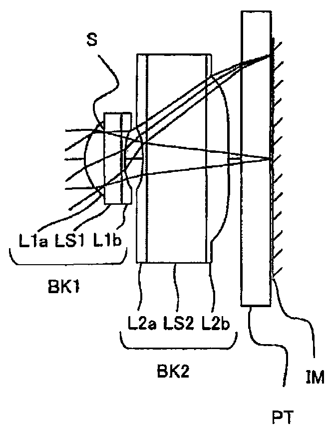
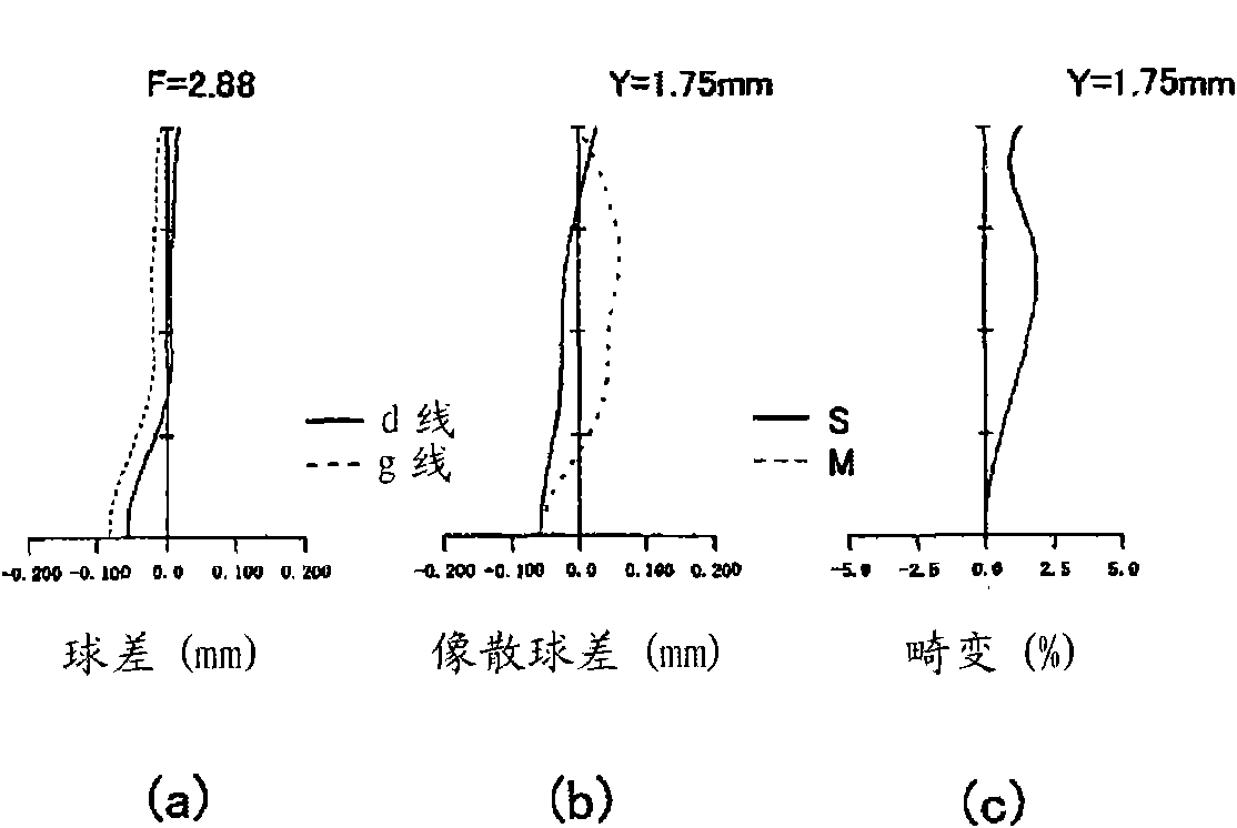
[0219] Table 1 shows the lens data of Example 1. Figure 6 It is a sectional view of the photographing lens shown in Example 1. Figure 7 It is an aberration diagram (spherical aberration (a), astigmatism (b), distortion (c)) of Example 1. Here, in the spherical aberration diagram, the solid line indicates the spherical aberration amount for the d-line, the dotted line indicates the spherical aberration amount for the g-line, and in the astigmatism diagram, the solid line indicates the sagittal plane, and the dotted line indicates the meridional plane (hereinafter same as in the aberration map). The photographing lens of Example 1 is provided in order from the object side: 1a lens portion L1a convex on the object side, aperture stop S, first lens substrate LS1, and 1b lens portion L1b concave on the image side 1st lens group BK1, followed by 2nd lens group BK2 consisting of 2a lens part L2a concave on the object side, 2nd lens substrate LS2, and 2b lens part L2b, and finally...

Embodiment 2

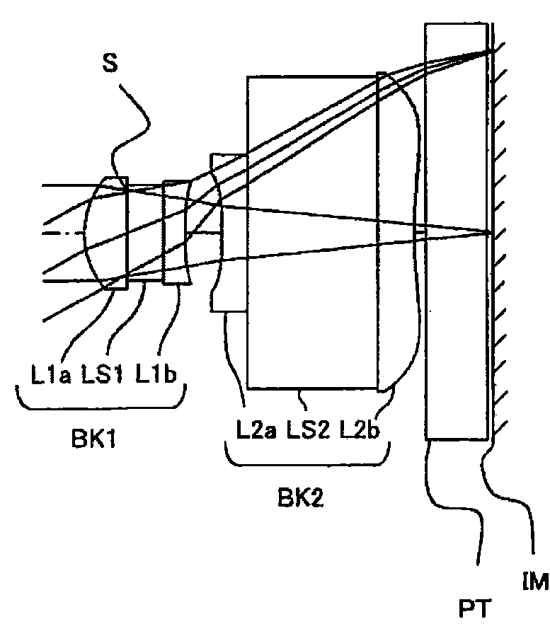
[0269] Table 2 shows the lens data of Example 2. Figure 8 It is a cross-sectional view of the photographic lens shown in Example 2. Figure 9 It is an aberration diagram (spherical aberration (a), astigmatism (b), distortion (c)) of Example 2. The photographing lens of Example 2 is provided in order from the object side: a 1a lens portion L1a convex on the object side, an aperture stop S, a first lens substrate LS1, and a 1b lens portion L1b concave on the image side 1st lens group BK1, followed by 2nd lens group BK2 consisting of 2a lens part L2a concave on the object side, 2nd lens substrate LS2, and 2b lens part L2b, and finally a hypothetical optical low-pass filter, Parallel plate PT for infrared cut filters, sealing glass for solid-state imaging devices, etc. IM is the imaging plane of the imaging element. In addition, all the surfaces of the lens portion that are in contact with air are aspherical.

[0270] In Example 2, the refractive index nI with respect to the ...

Embodiment 3

[0319] Table 3 shows the lens data of Example 3. Figure 10 It is a cross-sectional view of the photographing lens shown in Example 3. Figure 11 It is an aberration diagram (spherical aberration (a), astigmatism (b), distortion (c)) of Example 3. The photographic lens of Example 3 is provided in order from the object side: a 1a lens portion L1a convex on the object side, an aperture stop S, a first lens substrate LS1, and a 1b lens portion L1b concave on the image side 1st lens group BK1, followed by 2nd lens group BK2 consisting of 2a lens part L2a concave on the object side, 2nd lens substrate LS2, and 2b lens part L2b, and finally a hypothetical optical low-pass filter, Parallel plate PT for infrared cut filters, sealing glass for solid-state imaging devices, etc. IM is the imaging plane of the imaging element. In addition, all the surfaces of the lens portion that are in contact with air are aspherical.

[0320] In Example 3, the refractive index nI with respect to th...


PUM


Abstract

An image pickup lens includes: a first lens block with a positive power and a second lens block. The first lens block includes a first lens substrate, a lens portion 1a with a positive power, formed on an object-side surface of the first lens substrate, and a lens portion 1b with a negative power, formed on an image-side surface of the first lens substrate. The object-side surface of the lens portion 1a is a convex surface, and an image-side surface of the lens portion 1b is a concave surface. The second lens block includes a second lens substrate, and a lens portion 2a with a negative power, formed on an object-side surface of the second lens substrate. The object-side surface of the lens portion 2a is a concave surface. The image pickup lens satisfies the predetermined conditional expressions.

Description

technical field [0001] The present invention relates to an imaging lens for an imaging device using solid-state imaging elements such as a CCD (Charge Coupled Devices) image sensor and a CMOS (Complementary Metal-Oxide Semiconductor) image sensor. 1) A photographic lens of an optical system of a lens, a photographic device using the photographic lens, a portable terminal, a method of manufacturing the photographic lens, and a method of manufacturing the photographic device. Background technique [0002] The compact and thin imaging device is installed in compact and thin electronic equipment such as mobile phones and PDAs (Personal Digital Assistant), that is, portable terminals, whereby not only audio information but also image information can be exchanged to distant places. [0003] As imaging elements used in these imaging devices, solid-state imaging elements such as CCD image sensors and CMOS image sensors are used. In recent years, the high pixelation of imaging eleme...

Claims


Application Information

Patent Timeline
Patent Type & Authority Patents(China)
IPC IPC(8): G02B13/00G02B13/18H04N5/225
CPCG02B13/006H04N5/2254G02B13/003H04N23/55H04N25/611
Inventor 川崎贵志福田泰成松井一生
Owner KONICA MINOLTA INC
Why Eureka
Try Eureka