Method and system for etching wafer back

A crystal back and etching technology, applied in electrical components, semiconductor/solid-state device manufacturing, circuits, etc., can solve problems such as reducing the quality of semiconductor chips and discoloration of the front of the wafer

Inactive Publication Date: 2011-01-26
SEMICON MFG INT (SHANGHAI) CORP +1
View PDF0 Cites 0 Cited by
  • Summary
  • Abstract
  • Description
  • Claims
  • Application Information

AI Technical Summary

Problems solved by technology

[0011] However, when implementing the above etching method, the implementers found that the front of the wafer etched by t

Method used


Image

  • Method and system for etching wafer back
  • Method and system for etching wafer back
  • Method and system for etching wafer back

Examples


Embodiment Construction

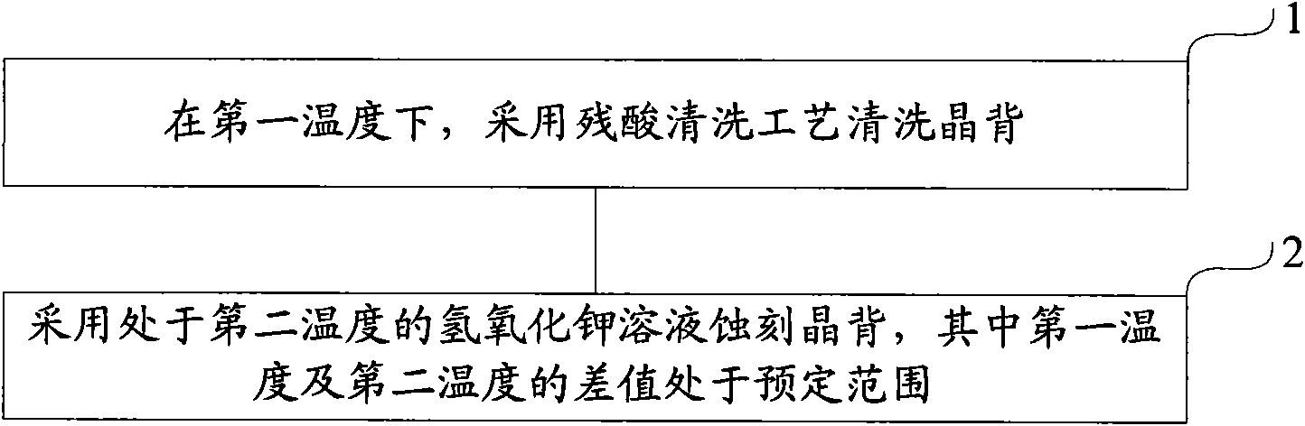
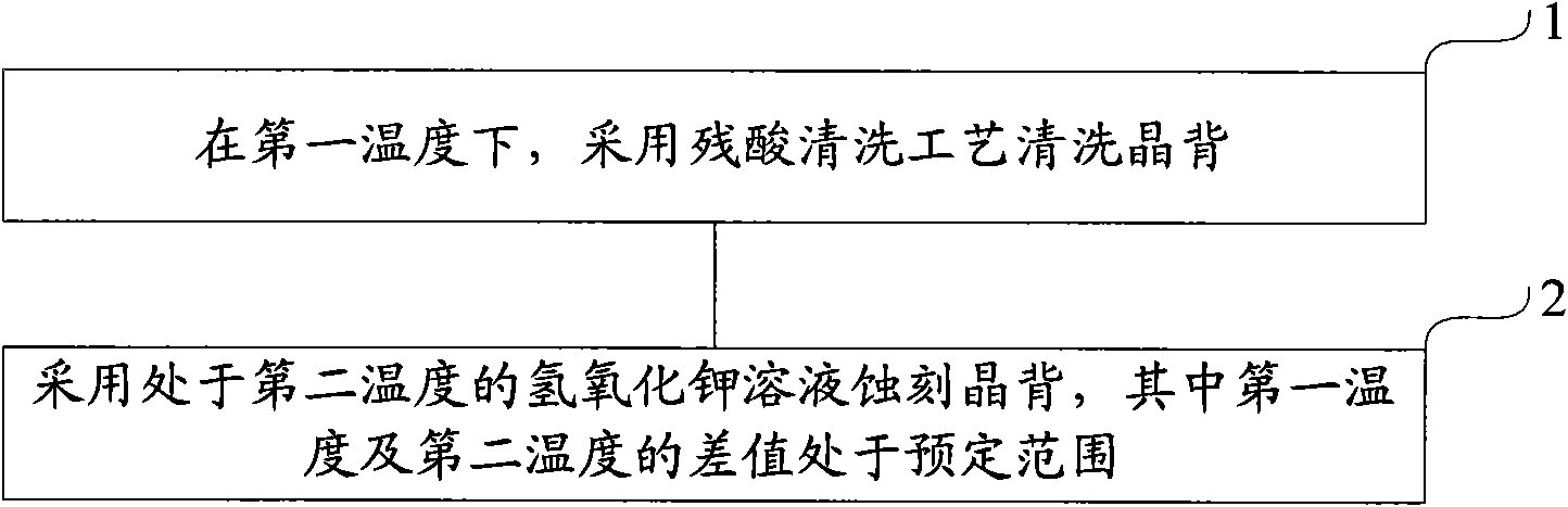
[0027] Aiming at the problem of discoloration of the front side of the wafer mentioned in the background technology, the inventors of the present application obtained by analyzing the existing crystal back etching process. Due to the large temperature difference in each step in this process, for example, the temperature of step a1 and step a2 changes from 60°C to The temperature from step a2 to step a3 increases from 23°C to 70°C, so that the acid-proof film attached to the front of the wafer expands with heat and contracts with cold, resulting in stretching and contraction, resulting in a gap between the acid-proof film and the glue. Cracks are formed or even separated, and the glue is used to bond the acid-proof film and the wafer. The acid from each step of the etching process will then enter the front side of the wafer through the above-mentioned cracks and separation cracks, forming residual acid or a by-product after the acid reacts with the wafer. In addition, through t...


PUM


Abstract

The invention provides a method and a system for etching a wafer back, avoiding a discoloration phenomenon on the front face of a wafer and improving the quality of the wafer by attaching an anti-acid membrane to the front face of the wafer corresponding to the back face of the wafer. The method comprises the following steps of: cleaning the back face of the wafer at a first temperature by adopting a reacted acid cleaning process; and etching the back face of the wafer with a potassium hydroxide solution at a second temperature, wherein the difference value of the first temperature and the second temperature is in a preset range.

Description

technical field [0001] The invention relates to the field of semiconductors, in particular to a crystal back etching method and system. Background technique [0002] When making semiconductor chips, the back of the wafer is usually rarely processed, but for power component chips such as power chips (Power IC, Power Integrated Circuit), it is usually necessary to grind and deposit metal on the back of the wafer. process to reduce the resistance of power components. [0003] Since the crystal back surface is usually relatively smooth, in order to increase the adhesion between the metal and the crystal back surface when depositing metal, the crystal back etching treatment is generally carried out to increase the roughness of the crystal back surface, which is beneficial to the deposited metal and crystal surface. Adhesion to the back enhances the deposition effect. [0004] The existing crystal back etching method is as follows: firstly, the acid-proof film is glued to the fr...

Claims


Application Information

Patent Timeline
IPC IPC(8): H01L21/306H01L21/00
Inventor 陈泰江吴昊
Owner SEMICON MFG INT (SHANGHAI) CORP
Why Eureka
Try Eureka