Failure detection method and device

A detection method and detection device technology, applied in the direction of measuring devices, semiconductor/solid-state device testing/measurement, electrical measurement, etc., can solve the problems that cannot meet the needs of small-scale failure analysis, low sensitivity and positioning accuracy of OBIRCH technology, and avoid thermal effects , to avoid size restrictions, to avoid the effect of damage

Inactive Publication Date: 2011-01-26
SEMICON MFG INT (SHANGHAI) CORP +1
View PDF0 Cites 17 Cited by
  • Summary
  • Abstract
  • Description
  • Claims
  • Application Information

AI Technical Summary

Problems solved by technology

[0006] However, OBIRCH technology is only suitable for large-scale defect location of semiconductor devices, and cannot meet the needs of small-scale failure analysis, especially when performing defect detection on narrow-sized metal interconnection lines, due to the limitation of laser spot size, OBIRCH technology has defects to find Sensitivity and positioning accuracy are too low

Method used


Image

  • Failure detection method and device
  • Failure detection method and device
  • Failure detection method and device

Examples


Embodiment Construction

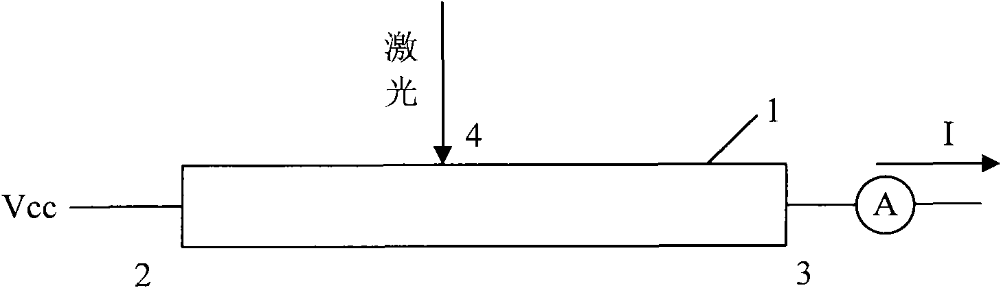
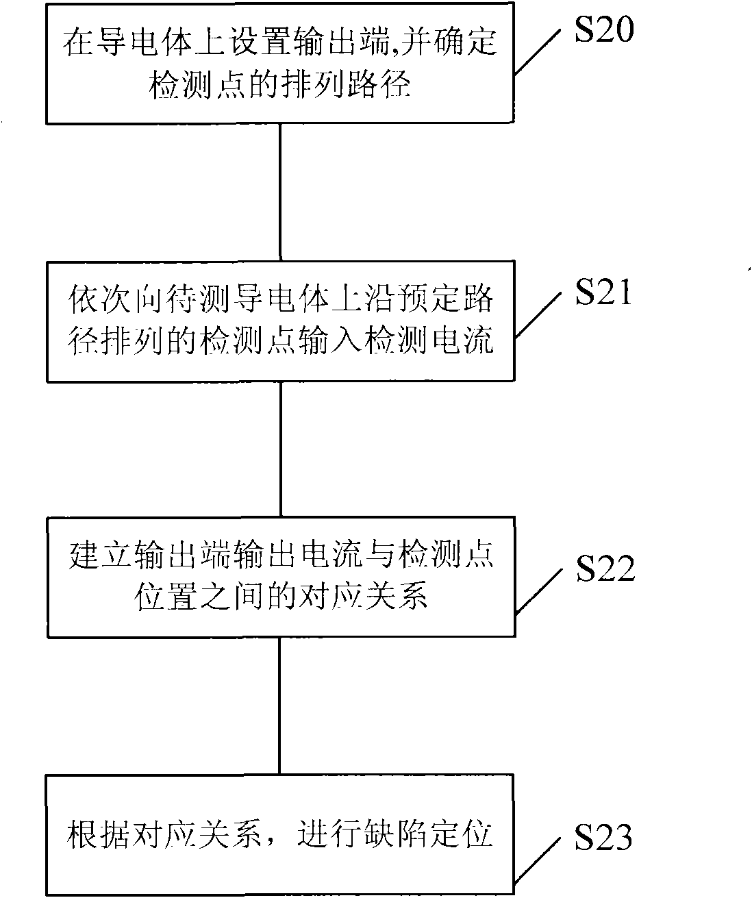
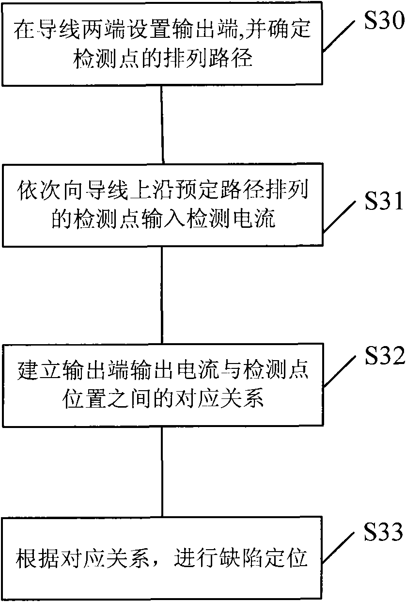
[0034] According to the law of conservation of charge, the sum of the output currents of the device is equal to the sum of the input currents. Therefore, if several output terminals with equal potential potentials are set on the conductor (that is, the potential potential of each output terminal is the same), and when the detection current is input on the conductor, all The sum of the currents at the output terminals is a constant value. Since the current always tends to the path with the least impedance, the current at each output terminal depends on the resistance between the output terminal and the detection point. When the position of the detection point changes, the current of each output terminal will also change accordingly. This change should be corresponding and unique, that is, when the same detection current is input at a fixed detection point, the output current of each output terminal should be Fixed, the output current of each output end forms a corresponding rel...


PUM


Abstract

A failure detection method and device are used for detecting defects on a conductor. The method comprises the following steps: arranging at least two output ends with equal electric potentials on the conductor to be detected; inputting constant detection current to the detection points arranged on the conductor to be detected along the preset path in sequence; detecting the output current of each output end; establishing the correspondence between the output current of the output ends and the positions of the detection points based on the position information of each detection point and the output current information of each output end; and judging whether the detection points have defects according to the correspondence. The method can accurately locate the defects and use charged particle beams as the detection current sources to avoid dimension limit of the irradiation points, thus meeting the requirement of small-dimension failure analysis.

Description

technical field [0001] The invention relates to the field of semiconductor manufacturing, in particular to a failure detection method and a failure detection device for metal interconnection lines in semiconductor devices. Background technique [0002] In the field of semiconductor manufacturing, failure analysis of semiconductor devices is a feedback process for improving the reliability and stability of process technology, which involves finding and correcting the root causes of defects to overcome the problems caused by defects. Proper failure analysis is critical to improving the quality of semiconductor devices. Incorrect failure analysis can lengthen the period required to develop and ramp up semiconductor device products. Generally, failure analysis includes external inspection, non-destructive analysis, electrical performance testing, destructive analysis, etc. [0003] In order to improve the integration of semiconductor devices, it is necessary to obtain as many ...

Claims


Application Information

Patent Timeline
Patent Type & Authority Applications(China)
IPC IPC(8): H01L21/66G01N27/00G01R19/00
CPCH01L22/12G01R31/307G01R31/2853H01L2924/0002H01L2924/00
Inventor 龚斌郭强
Owner SEMICON MFG INT (SHANGHAI) CORP
Why Eureka
Try Eureka