Double wafer carrier process for creating integrated circuit die with through-silicon vias and micro-electro-mechanical systems protected by a hermetic cavity created at the wafer level

a carrier process and integrated circuit technology, applied in semiconductor devices, semiconductor/solid-state device details, electrical apparatus, etc., can solve the problems of incompatibility with the mechanical and chemical fragility of the mems structure, the current separate processing of the product wafer prior to packaging is time-consuming, and the current satisfactory way of handling the product wafer is incompatible with the structure. , to achieve the effect of preventing further size reduction of certain devices

Active Publication Date: 2011-06-14
TEXAS INSTR INC
View PDF2 Cites 23 Cited by
  • Summary
  • Abstract
  • Description
  • Claims
  • Application Information

AI Technical Summary

Benefits of technology

[0005]Applicants have realized that the current separate processing of wafers prior to packaging can be time consuming, and can prevent further size reduction for certain devices. It is Applicants solution to process both sides of a product wafer, thereby significantly reducing, and even eliminating, a necessity to package multiple and separately processed wafers in a package.
[0007]The Applicants observed, for example in a micro-electro-mechanical system (MEMS), that a hermetic cavity can be required in wafer form to protect the MEMS devices during subsequent assembly. In addition, through-silicon-vias (TSVs) are desirable with MEMS in a wafer level hermetic cavity because this approach significantly reduces the size of the die with MEMS, reduces the packaged unit size, and improves the interconnect performance. However, the MEMS device and the wafer level hermetic cavity structures have maximum temperature constraints and mechanical support requirements during the TSV process flow which are incompatible with some TSV process flows.
[0009]Certain process flow sequences must occur in all standard TSV processing and in standard MEMS flow with a wafer lever hermetic cavity. The Applicants have discovered a process for managing and handling a product wafer without damaging a processed side of the wafer, and without disrupting known process flows. The inventive process can utilize and be implemented with all known process flows, for example forming TSVs, forming MEMS, and forming a hermitic cavity over the MEMS structure, all on the same substrate, and without damaging any of the processed components.

Problems solved by technology

Applicants have realized that the current separate processing of wafers prior to packaging can be time consuming, and can prevent further size reduction for certain devices.
Based upon current known techniques and apparatus for handling product wafers, there is currently no satisfactory way to handle the product wafer and process the product wafer on both sides without damaging the processed side of that wafer.
However, the MEMS device and the wafer level hermetic cavity structures have maximum temperature constraints and mechanical support requirements during the TSV process flow which are incompatible with some TSV process flows.
However, this mechanical contact has been found to scratch the MEMS cavity materials and can further be incompatible with the mechanical and chemical fragility of the MEMS structure.

Method used


Image

  • Double wafer carrier process for creating integrated circuit die with through-silicon vias and micro-electro-mechanical systems protected by a hermetic cavity created at the wafer level
  • Double wafer carrier process for creating integrated circuit die with through-silicon vias and micro-electro-mechanical systems protected by a hermetic cavity created at the wafer level
  • Double wafer carrier process for creating integrated circuit die with through-silicon vias and micro-electro-mechanical systems protected by a hermetic cavity created at the wafer level

Examples


Embodiment Construction

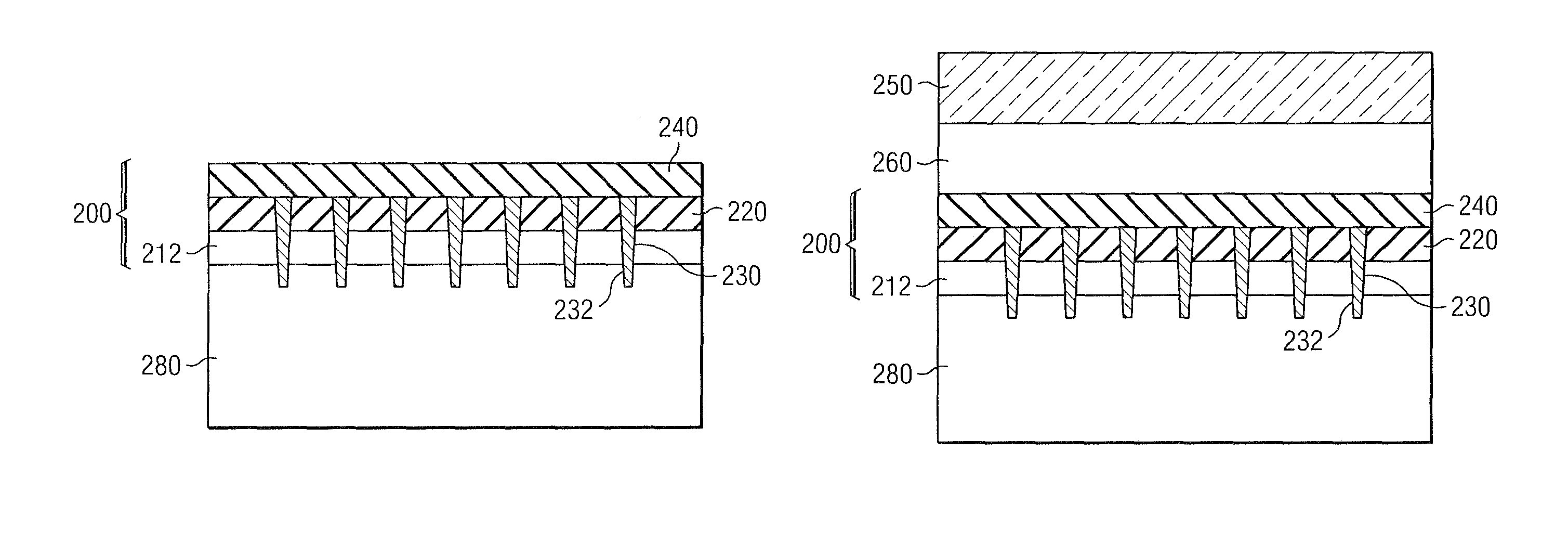
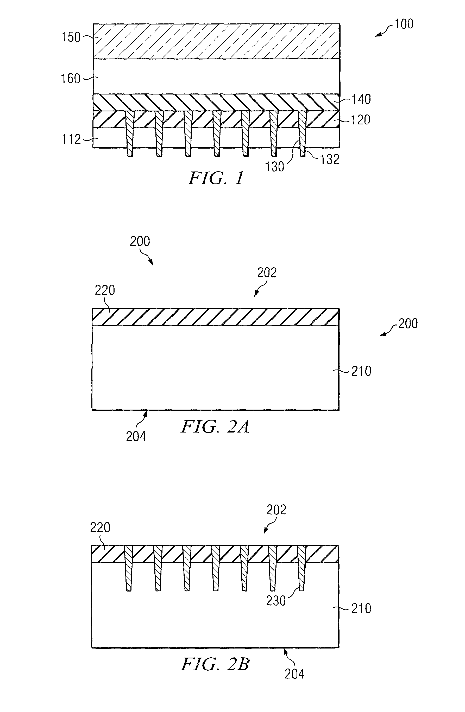
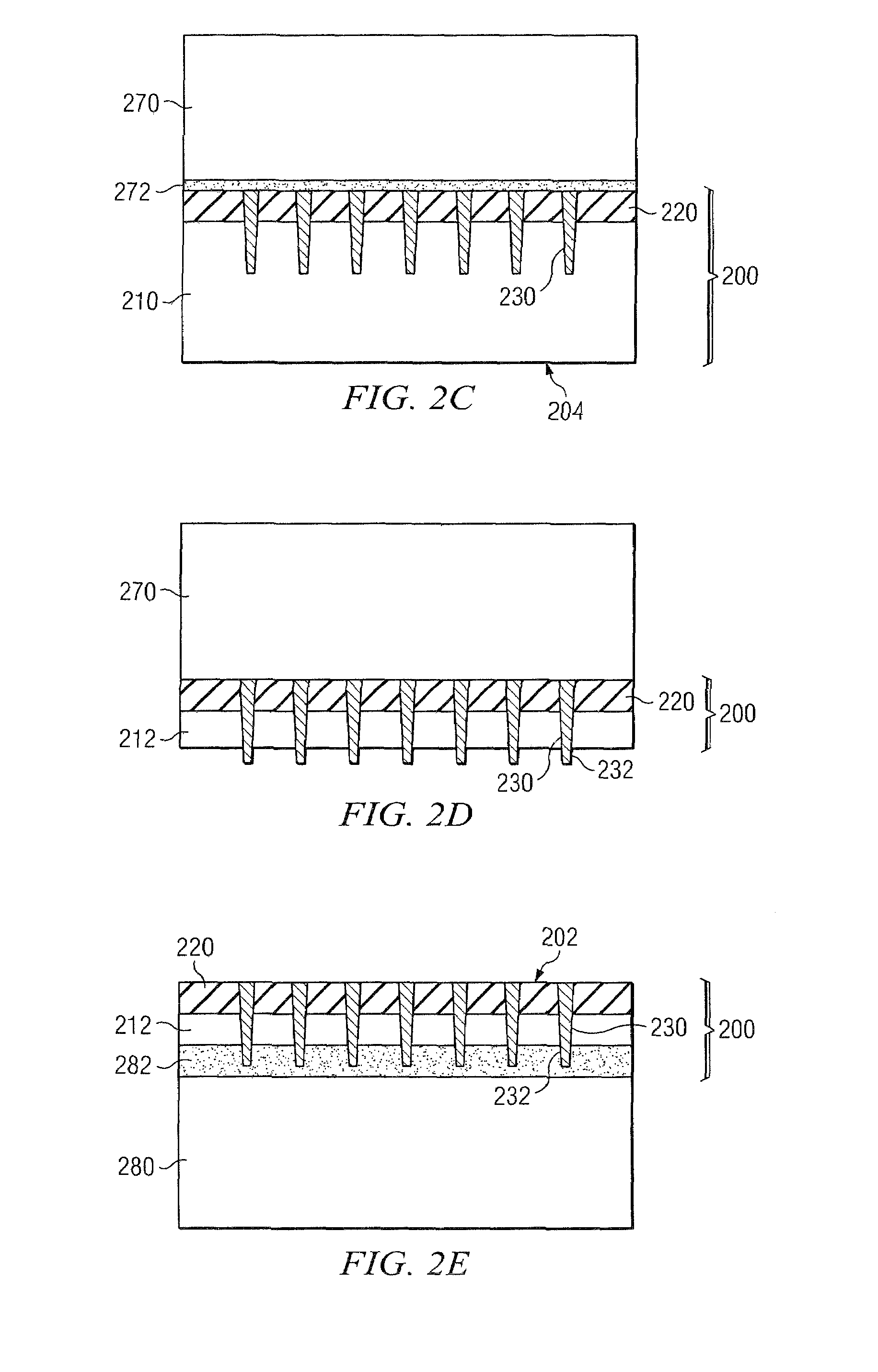
[0017]Reference will now be made in detail to the exemplary embodiments of the present disclosure, an example of which is illustrated in the accompanying drawings. Wherever possible, the same reference numbers will be used throughout the drawings to refer to the same or like parts.

[0018]In the following description, reference is made to the accompanying drawings that form a part thereof, and in which is shown by way of illustration specific exemplary embodiments which may be practiced. These embodiments are described in sufficient detail to enable those skilled in the art to practice the embodiments and it is to be understood that other embodiments may be utilized and that changes may be made without departing from the scope of the invention. The following description is, therefore, merely exemplary.

[0019]Notwithstanding that the numerical ranges and parameters setting forth the broad scope of the disclosure are approximations, the numerical values set forth in the specific examples...


PUM


Abstract

A TSV-MEMS packaging process is provided. The process includes forming TSVs in the front side of the product wafer, and attaching a first carrier to the front side of the product wafer, subsequent to forming TSVs. The process further includes thinning the back side of the product wafer to expose TSV tips, detaching the first carrier from the front side of the product wafer, and transferring the thinned wafer to a second carrier with back side adhered to the second wafer carrier. Semiconductor components are added to the front side of the product wafer, followed by forming a hermetic cavity over the added semiconductor components, and detaching the second carrier from the back side of the product wafer. Wafer level processing continues after detaching the second carrier.

Description

[0001]This application claims priority from U.S. Provisional Patent Application Ser. No. 61 / 052,517, filed May 12, 2008, which is hereby incorporated by reference in its entirety.FIELD[0002]This invention relates generally to a carrier concept for processing a semiconductor device, and more particularly sequentially processing both sides of a product wafer using carriers supporting opposing sides of the product wafer at different times during processing.BACKGROUND[0003]In the field of semiconductor packaging, it is standard in the industry to process only one side of each of several wafers, and then combine the separately processed wafers together in packaging.[0004]For example, a known MEMS fuel cell uses three substrates in the final product. One substrate is a silicon wafer which has the MEMS device and one substrate is a glass plate which has through silicon vias (TSVs) formed therein. Separate processing of the wafers prior to packaging is common because each die component can ...

Claims


Application Information

Patent Timeline
Patent Type & Authority Patents(United States)
IPC IPC(8): H01L23/52
CPCB81C1/0023H01L21/6835H01L21/76898B81B2207/096H01L2924/14B81C2201/0191
Inventor BONIFIELD, THOMAS DYERWINTER, THOMAS W.MORRISON, WILLIAM R.WINTERTON, GREGORY D.HAIDER, ASAD M.
Owner TEXAS INSTR INC
Why Eureka
Try Eureka