Semiconductor Laser Apparatus

a laser apparatus and semiconductor technology, applied in the direction of lasers, semiconductor laser arrangements, semiconductor lasers, etc., can solve the problems of inconvenient pickup, inability to integrate blue-violet semiconductor laser devices with infrared and red semiconductor laser devices in one chip, and difficulty in simplifying the configuration or price reduction of pickups, etc., to achieve easy adjustment and increase the diameter of individual vias

Inactive Publication Date: 2011-08-04
SANYO ELECTRIC CO LTD
View PDF4 Cites 23 Cited by
  • Summary
  • Abstract
  • Description
  • Claims
  • Application Information

AI Technical Summary

Benefits of technology

[0047]In the aforementioned method of manufacturing the semiconductor laser apparatus, the step of forming the second semiconductor laser device preferably includes a step of the second semiconductor laser device having the third surface on a surface of a growth substrate and further includes a step of forming the fourth surface on the second semiconductor laser device by removing the growth substrate in a region overlapping with at least the first semiconductor laser device to reduce a thickness of the second semiconductor laser device in advance of the step of so arranging the first semiconductor laser device with respect to the second semiconductor laser device that the part of the first surface or the second surface overlaps with the fourth surface. According to this structure, a thickness (thickness from the third surface to the fourth surface) of the laser device in a region of the second semiconductor laser device overlapping with the part of the first surface of the first semiconductor laser device is reduced, and hence the first semiconductor laser device and the second semiconductor laser device can be arranged on the same support substrate in a state where the part of the first surface of the first semiconductor laser device easily overlaps with the fourth surface of the second semiconductor laser device. Thus, a height from the support substrate to an active layer of the first semiconductor laser device and a height from the support substrate to an active layer of the second semiconductor laser device can be easily adjusted, and hence the semiconductor laser apparatus where laser beam-emitting points of the both laser devices are closed to each other can be obtained. Thus, when this semiconductor laser apparatus is applied to an optical pickup, light emitted from each of the semiconductor laser devices can be incident at substantially the same angle with respect to (in a direction perpendicular to) a recording surface of an optical disk, a DVD or the like, and hence optical spot quality of the semiconductor laser device in each recording medium can be inhibited from dispersion.
[0048]In the aforementioned method of manufacturing the semiconductor laser apparatus, the via preferably includes a first via and a second via so formed in the support substrate as to be connected to at least either the first semiconductor laser device or the second semiconductor laser device, and a first distance between a first facet of the support substrate and a center position of the first via along a direction in which a waveguide of the first semiconductor laser device extends and a second distance between the first facet of the support substrate and a center position of the second via along a direction in which a waveguide of the first semiconductor laser device extends are different from each other. According to this structure, the first via and the second via can be formed deviating to each other along a cavity direction of the laser device, and hence a plurality of the vias can be efficiently provided in the support substrate while increasing diameters of the individual vias even when the support substrate having a small width is employed.

Problems solved by technology

However, these methods cause increase of the number of components, and hence downsizing, simplified configuration or price-reduction of the pickup is disadvantageously difficult.
On the other hand, the blue-violet laser is not formed on a GaAs substrate, and hence it is very difficult to integrate the blue-violet semiconductor laser device together with the infrared and red semiconductor laser devices in one chip.
However, in the semiconductor laser device disclosed in Japanese Patent Laying-Open No. 2004-207480, the respective surfaces of the light emitting element layers at the opposite sides of the light emitting elements to the substrates are bonded to be opposed to each other, and hence a size (thickness) of the semiconductor laser device is disadvantageously increased due to addition of a thickness of the second light emitting element to a thickness of the first light emitting element.
Thus, the width of each of the light emitting elements narrows, whereby it is disadvantageously difficult to bond a metal wire or the like to each of the light emitting elements.
Also in the semiconductor laser apparatus disclosed in Japanese Patent Laying-Open No. 2005-317919, the respective surfaces of the laser device layers at the opposite sides of the laser devices to the substrates are bonded to be opposed to each other, and hence a size (thickness) of the semiconductor laser apparatus is disadvantageously increased due to addition of a thickness of the red (or infrared) semiconductor laser device to a thickness of the blue-violet semiconductor laser device.
Thus, the width of each of the laser devices narrows, whereby it is disadvantageously difficult to bond a metal wire or the like to each of the laser devices.

Method used


Image

  • Semiconductor Laser Apparatus
  • Semiconductor Laser Apparatus
  • Semiconductor Laser Apparatus

Examples


first embodiment

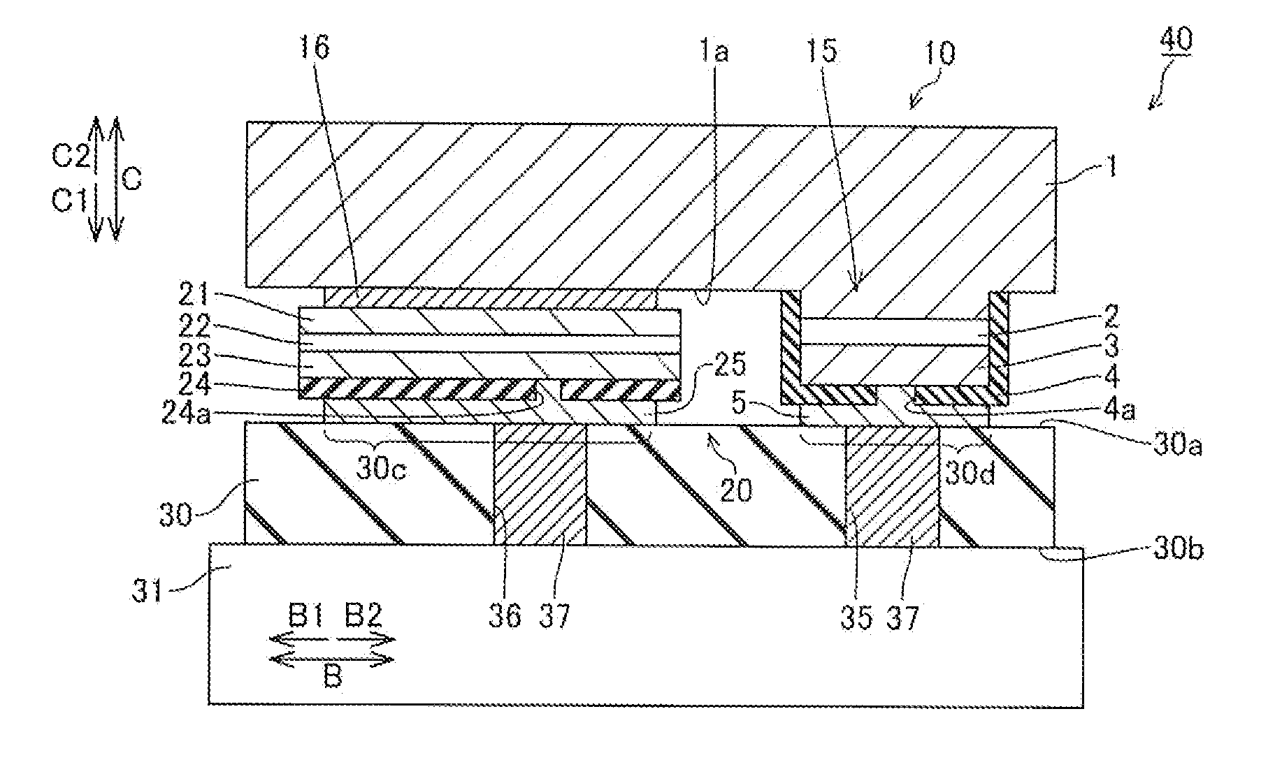
[0135]A structure of a semiconductor laser apparatus 100 according to a first embodiment of the present invention is described with reference to FIGS. 7 and 8. FIG. 7 shows a section taken along the line 1000-1000 in FIG. 8.

[0136]The semiconductor laser apparatus 100 has a structure in which a blue-violet semiconductor laser device 50 and a two-wavelength laser device 60 are bonded onto a surface of a support substrate 101 made of insulating Si to be adjacent to each other in a lateral direction (direction B), as shown in FIG. 7. The blue-violet semiconductor laser device 50 has a lasing wavelength of about 405 nm and a cavity length of about 800 μm. The two-wavelength laser device 60 is monolithically formed with a red semiconductor laser device 70 having a lasing wavelength of about 650 nm and a cavity length of about 1.5 mm and an infrared semiconductor laser device 80 having a lasing wavelength of about 780 nm and a cavity length of about 1.5 mm. The blue-violet semiconductor la...

first modification

of First Embodiment

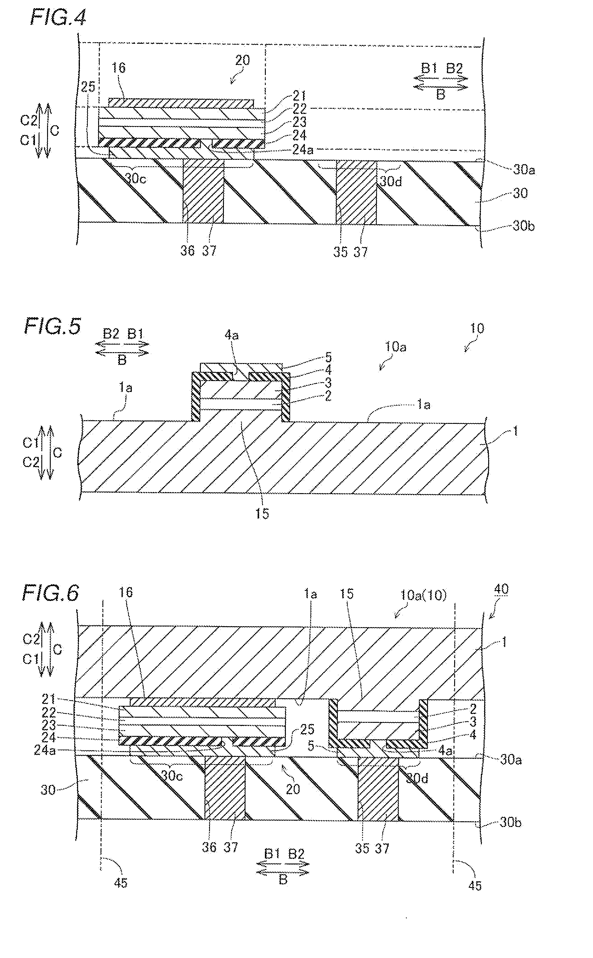
[0194]A first modification of the first embodiment is described with reference to FIG. 14. According to the first modification, a GaAs substrate 65 partly remains in a two-wavelength laser device 60a brought into a chip state, dissimilarly to the first embodiment. In the figure, a structure similar to that of the semiconductor laser apparatus 100 according to the first embodiment is denoted by the same reference numerals. The two-wavelength laser device 60a is an example of the “integrated laser device” in the present invention.

[0195]In a semiconductor laser apparatus 100a according to the first modification, as shown in FIG. 14, an n-side ohmic electrode 62 and an n-side pad electrode 63 for conducting with an n-type GaN substrate 51 of a blue-violet semiconductor laser device 50 are formed on an upper surface of an n-type contact layer 61 formed with a red semiconductor laser device 70 on the lower portion in the two-wavelength laser device 60a. The GaAs substra...

second modification

of First Embodiment

[0198]A second modification of the first embodiment is described with reference to FIGS. 15 and 16. According to the second modification, pad electrodes 92 and 93 for bonding a two-wavelength laser device 60 are formed on an n-type Si support substrate 130 having conductivity through an insulating film 131 made of SiO2 dissimilarly to the first embodiment. FIG. 15 shows a section taken along the line 1100-1100 in FIG. 16. In the figures, a structure similar to that of the semiconductor laser apparatus 100 according to the first embodiment is denoted by the same reference numerals. The Si support substrate 130 is an example of the “support substrate” in the present invention.

[0199]In a semiconductor laser apparatus 100b according to the second modification, a blue-violet semiconductor laser device 50 and the two-wavelength laser device 60 are bonded onto a surface of the n-type Si support substrate 130 having conductivity to be adjacent to each other, as shown in F...


PUM


Abstract

This semiconductor laser apparatus includes a first semiconductor laser device having a first surface and a second surface, an integrated laser device formed by a second semiconductor laser device and a third semiconductor laser device having a third surface and a fourth surface, and a support substrate. The third surface is bonded onto a first region of the support substrate, a first section of the first surface overlaps with at least part of the fourth surface, and a second section of the first surface is bonded to a second region of the support substrate.

Description

CROSS-REFERENCE TO RELATED APPLICATION[0001]The priority application numbers JP2010-23313, Method of Manufacturing Semiconductor Laser Apparatus and Semiconductor Laser Apparatus, Feb. 4, 2010, Masayuki Hata et al., and JP2010-40128, Method of Manufacturing Semiconductor Laser. Apparatus and Semiconductor Laser Apparatus, Feb. 25, 2010, Masayuki Hata et al., upon which this patent application is based are hereby incorporated by reference.BACKGROUND OF THE INVENTION[0002]1. Field of the Invention[0003]The present invention relates to a semiconductor laser apparatus, and more particularly, it relates to a semiconductor laser apparatus having a plurality of semiconductor laser devices bonded to each other.[0004]2. Description of the Background Art[0005]An infrared semiconductor laser device having a wavelength of about 180 nm has been employed as a light source for a CE) (compact: disc) / CD-R (compact disc-recordable) drive in general. A red semiconductor laser device having a wavelengt...

Claims


Application Information

Patent Timeline
Patent Type & Authority Applications(United States)
IPC IPC(8): H01S5/40H01S5/323
CPCH01S5/40H01S5/323H01S5/0237H01S5/02345H01S5/0234H01S5/04256H01S5/02326H01S5/4087H01S5/02375H01S5/4031H01L2924/00014H01L2224/48091
Inventor HATA, MASAYUKINOMURA, YASUHIKOBESSHO, YASUYUKI
Owner SANYO ELECTRIC CO LTD
Why Eureka
Try Eureka