Method of manufacturing semiconductor device

a manufacturing method and semiconductor technology, applied in the direction of semiconductor/solid-state device manufacturing, solid-state devices, electric devices, etc., can solve the problems of increased manufacturing process cost, difficult to etch copper, and decreased device performance, so as to reduce manufacturing process steps and reduce manufacturing process cost

Active Publication Date: 2005-10-20
NEXCHIP SEMICON CO LTD
View PDF8 Cites 22 Cited by
  • Summary
  • Abstract
  • Description
  • Claims
  • Application Information

AI Technical Summary

Benefits of technology

[0017] Accordingly, at least one objective of the present invention is to provide a method of manufacturing a semiconductor device, wherein a metal-insulator-metal capacitor can be formed by using metal damascene process so as to decrease the steps of manufacturing process and to reduce the cost of the manufacturing process.
[0019] Because the metal deposition process is only performed once when the MIM capacitor and the dual metal damascene structure are formed simultaneously. Hence, the steps of manufacturing process can be decreased so that the cost of the manufacturing process is reduced. Moreover, during the formation of the dual damascene opening, the etching stop layer is used as a self-align mask. Therefore, the trench and the via hole can be formed by performing the etching process one time. Further, no capacitor dielectric layer is formed in the via hole so as to prevent the size of the via hole from being minimized.

Problems solved by technology

However, it is not easy to etch copper.
Therefore, the leakage of the metal wires will happen easily and the performance of the device is decreased.
Because it is necessary to perform several times of metal deposition process, chemical mechanical polishing process and photolithography process, the cost of the manufacturing process is increased.

Method used


Image

  • Method of manufacturing semiconductor device
  • Method of manufacturing semiconductor device
  • Method of manufacturing semiconductor device

Examples


Embodiment Construction

[0025] Reference will now be made in detail to the present preferred embodiments of the invention, examples of which are illustrated in the accompanying drawings. Wherever possible, the same reference numbers are used in the drawings and the description to refer to the same or like parts.

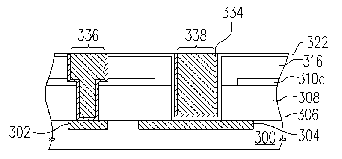
[0026]FIG. 3A through FIG. 3F are cross-sectional views showing a method of manufacturing a semiconductor device according to a preferred embodiment of the present invention.

[0027] As shown in FIG. 3A, a substrate 300 having a metal layer 302 and a metal layer 304 formed thereon is provided. The metal layer 302 and the metal layer 304 can be made of, for example, copper or aluminum.

[0028] A sealing layer 306 is formed over the substrate to cover the metal layer 302 and the metal layer 304. The sealing layer 306 can be made of, for example, silicon nitride or other proper nitride material or oxide material in order to prevent the surface of the metal layer 302 and the metal layer 304 from being ox...


PUM

PropertyMeasurementUnit
aspect ratioaaaaaaaaaa
conductiveaaaaaaaaaa
dielectricaaaaaaaaaa

Abstract

A method of manufacturing a semiconductor device. The method comprises steps of providing a substrate having a first metal layer and a second metal layer formed thereon. A first dielectric layer, an etching stop layer having a first opening located above the first metal layer and a second opening located above the second metal layer and a second dielectric layer are formed sequentially. A portion of the first dielectric layer and a portion of the second dielectric layer are removed to form a first trench exposing the first metal layer. A capacitor dielectric layer is formed over the substrate. A third opening is formed in the capacitor dielectric layer. A portion of the second dielectric layer and a portion of the first dielectric layer exposed by the third opening are removed to form an opening. A metal layer is formed to fill out the first trench and the opening.

Description

CROSS-REFERENCE TO RELATED APPLICATION [0001] This application claims the priority benefit of Taiwan application serial no. 93110944, filed on Apr. 20, 2004. BACKGROUND OF THE INVENTION [0002] 1. Field of Invention [0003] The present invention relates to a method of manufacturing a semiconductor device. More particularly, the present invention relates to a method of manufacturing a semiconductor device for simultaneously forming a dual metal damascene structure and a metal-insulator-metal capacitor. [0004] 2. Description of Related Art [0005] With the increase of the integration of the semiconductor device, in the deep sub-micron process, the size of the device is reduced and the space for forming the capacitor is decreased as well. The capacitance of a capacitor depends on the surface area of the upper electrode and the lower electrode. Currently, the way to increase the capacitance of the capacitor with the decrease of the size of the capacitor includes selecting a dielectric laye...

Claims


Application Information

Patent Timeline
Patent Type & Authority Applications(United States)
IPC IPC(8): H01L21/02H01L21/4763H01L21/76H01L21/768H01L23/522H01L23/532
CPCH01L21/76802H01L21/76808H01L21/7681H01L23/5223H01L23/5226H01L2924/0002H01L23/53295H01L28/55H01L2924/00
Inventor CHANG, KO-HSINGHUANG, CHIU-TSUNG
Owner NEXCHIP SEMICON CO LTD
Why Eureka
Try Eureka