

Plasma processing apparatus
A plasma and treatment device technology, applied in the field of plasma treatment devices, can solve the problems of electrode damage, shape deformation of discharge space, electrode deformation, etc., and achieves the effects of not easy insulation breakdown, improved stability, and suppression of deformation.
- Summary
- Abstract
- Description
- Claims
- Application Information
AI Technical Summary
Problems solved by technology
Method used
Image

Examples
Embodiment approach 1
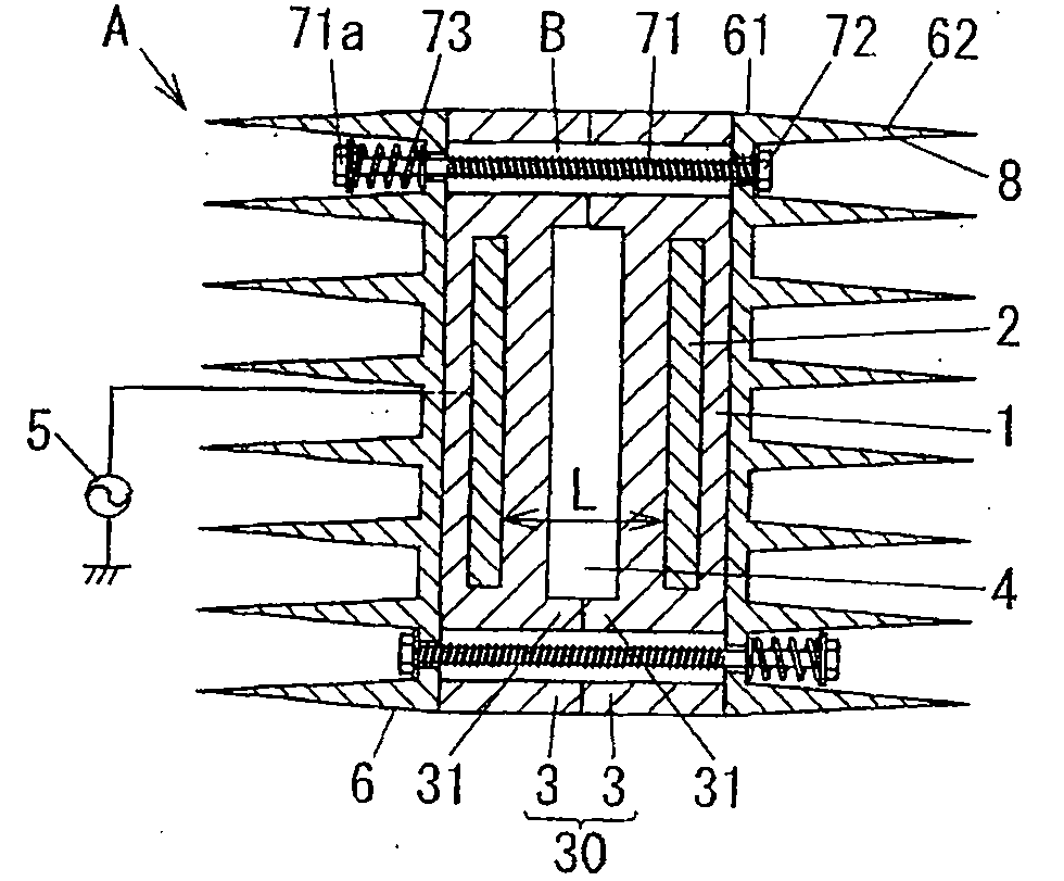
[0062] refer to Figure 1 to Figure 5(a) , FIG. 5(b) to describe the first embodiment of the present invention. The up and down directions in the following descriptions correspond to figure 2 in the up and down direction.
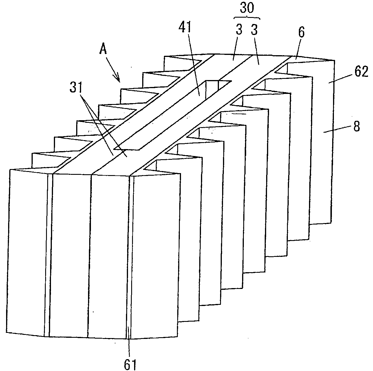
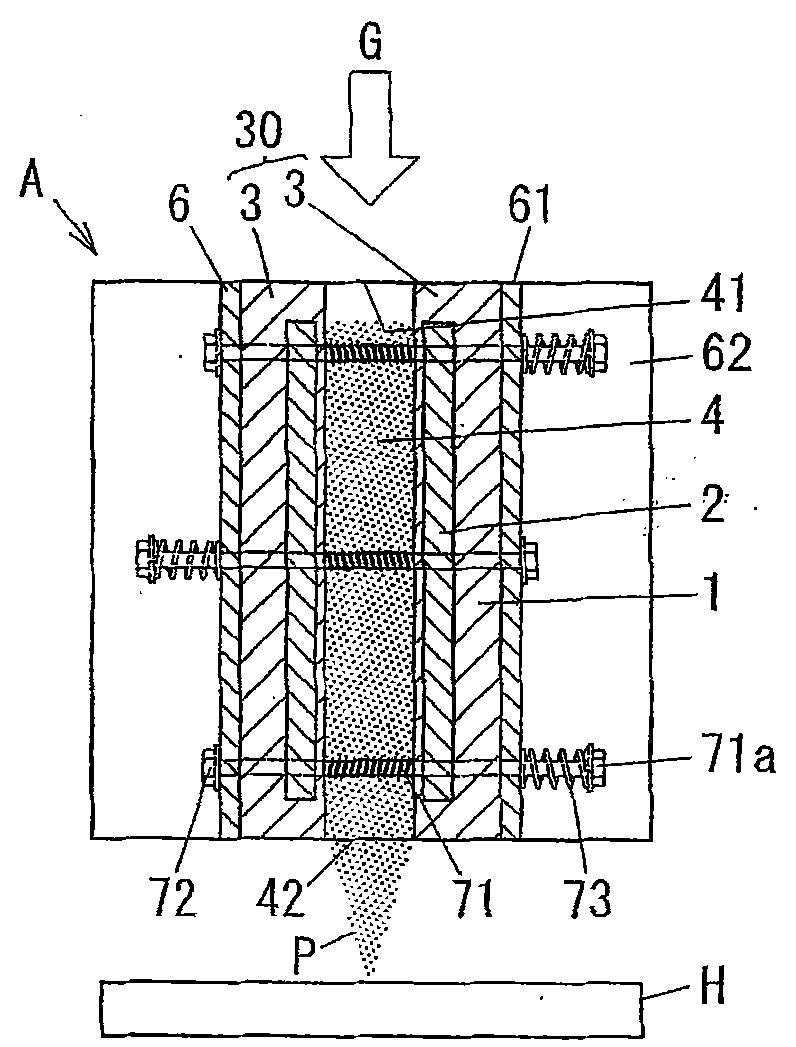
[0063] figure 1 , figure 2 An example of the plasma processing apparatus A of this embodiment is shown. This plasma processing apparatus A includes a discharge vessel 30 composed of a plurality of coated electrodes 3 facing each other, a power source 5, and a heat sink 6 .
[0064] The covered electrode 3 is formed by embedding the conductive layer 2 in a substantially flat insulating substrate (multilayer substrate) 1 . The insulating substrate 1 is a substrate formed by a ceramic (ceramic) sintered body of an insulating material (dielectric material) with a high melting point. Mullite, aluminum nitride, and other high-heat-resistant, high-strength ceramic sintered bodies are formed, but are not limited to these materials. It is particularly prefe...
Embodiment approach 2
[0087] refer to Figure 6 Next, a second embodiment of the present invention will be described. In this embodiment, a cooling fan (fan) 63 is provided around the heat dissipation fins 62 as cooling means, and other configurations are the same as in the first embodiment. Components common to those in Embodiment 1 are denoted by the same reference numerals and descriptions thereof are omitted.
[0088] In this embodiment, the cooling fan 63 is provided so as to face the heat dissipation fins 62 . In the present embodiment, by operating the cooling fan 63, the coated electrode 3 can be cooled more efficiently and the coated electrode 3 can be cooled more efficiently than only the cooling fins 62 are used to cool the coated electrode 3. The possibility that the cover electrode 3 is damaged or the like is reduced. It should be noted that the operation and stop of the cooling fan 63 can be controlled as necessary based on the measurement result of the temperature of the insulatin...
Embodiment approach 3
[0090] refer to Figure 7 Next, a third embodiment of the present invention will be described. In this embodiment, the heat sink 6 is formed with a cooling jacket 64 instead of the contact portion 61 and the heat radiation fin 62 , and other configurations are the same as those of the first embodiment. Components common to those in Embodiment 1 are denoted by the same reference numerals and descriptions thereof are omitted.
[0091] Such as Figure 7 As shown, the cooling jacket 64 of this embodiment is also pierced with a positioning hole B communicating with the spacer portion 31 of the coated electrode 3 . Furthermore, as in the first embodiment, the covered electrode 3 and the cooling jacket 64 are brought into pressure contact with each other by the bolt 71 , the nut 72 and the coil spring 73 .
[0092] The cooling jacket 64 is formed in a plate shape with the same material as the heat dissipation fins 62 in Embodiment 1, and a circulation path for circulating a refrig...
PUM
| Property | Measurement | Unit |
|---|---|---|
| Thickness | aaaaa | aaaaa |
| Thickness | aaaaa | aaaaa |
Abstract
Description
Claims
Application Information