
Super-thick copper circuit board solder resisting processing method

A processing method and circuit board technology, applied in the directions of printed circuit, printed circuit manufacturing, printed circuit secondary processing, etc., can solve the problems of increasing the brushing process, electrical corrosion, high cost of filling resin, shortening the production process, reducing Production cost, effect of avoiding bubble problems

Inactive Publication Date: 2011-01-26
大连太平洋多层线路板有限公司
View PDF5 Cites 40 Cited by
  • Summary
  • Abstract
  • Description
  • Claims
  • Application Information

AI Technical Summary

Problems solved by technology

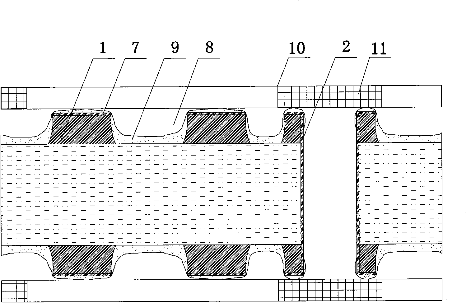
[0004] 1. The planar printing method can only process boards with a copper thickness below 6oz. When the copper thickness is greater than 6oz, the screen printing can only print ink on the protruding copper surface, and the substrate is more than 6oz (210μm) lower than the copper , because the height difference is too large, the pressure of the screen plate cannot reach the base material at all, so the base material cannot or can hardly be covered with ink, and for the solder mask printing of thick copper plate, the root of the line or between the lines must be filled in the first pass The ink plays a supporting role, so that the corners of the lines that have become relatively smooth can be covered with ink in the second printing, and then reach a certain thickness
[0005] 2. When using planar printing to process thick copper plates below 6oz, because the copper is thicker, the air bubbles between the lines cannot be completely eliminated, which will cause a large number of air bubbles and cracks in the solder mask between the lines after board printing, which will seriously affect For the performance of the circuit board, the customer had serious electrical corrosion during the withstand voltage test, and could not pass the customer's performance test
This method also has the disadvantage that it can only process boards with a copper thickness of less than 6oz. If the copper is thicker, the distance between the printed substrate and the screen plate is too large to be filled with resin; In addition to the problem of air bubbles, there is also the problem of increasing the brushing process and the high cost of filling resin, and it cannot be used in batches
[0007] The third processing method is to print the corners of the circuit by printing flat solder mask graphics first, and after a certain thickness of ink has accumulated at the root of the circuit, the second pass of solder mask is processed by electrostatic spraying ink. Boards smaller than 6oz are basically feasible, but when the copper thickness reaches 7oz and above, it is not feasible to print the corners of the circuit in the same way as above.
[0008] Today, when people regard car safety as the most important indicator for buying a car, the quality and safety of circuit boards is also our goal. The circuit boards we produce may experience various complex climate and geographical conditions. Copper power board, the current passing through it is ten times or even dozens of times larger than that of ordinary circuit boards, so it has strict requirements on the ink thickness of the lines, especially the corners, which must be greater than 8μm; and it is required that there should be no defects such as bubbles and cracks between the lines ;Once the above-mentioned defects exist, the customer will not be able to pass the withstand voltage and electric corrosion tests. Even if they pass by luck, it will bring great hidden dangers to the quality of the car

Method used


Image

  • Super-thick copper circuit board solder resisting processing method
  • Super-thick copper circuit board solder resisting processing method
  • Super-thick copper circuit board solder resisting processing method

Examples


Embodiment Construction

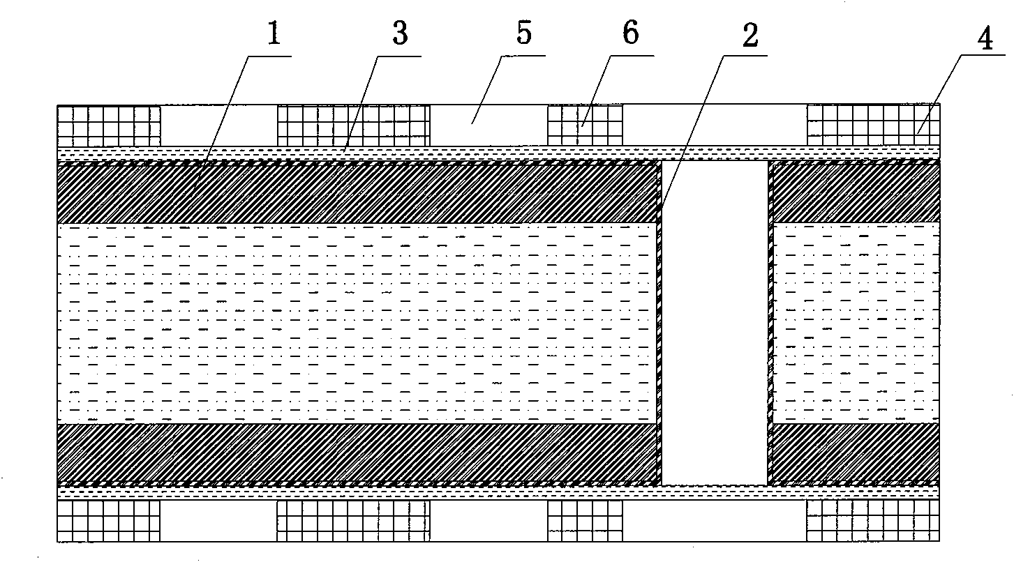
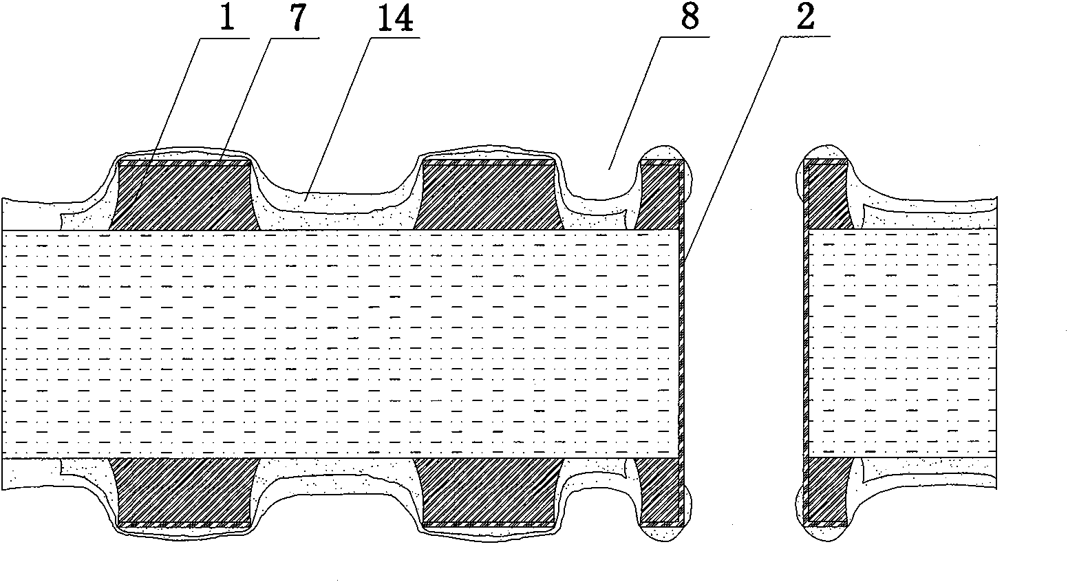
[0043] The present invention mainly adopts the current popular electrostatic spraying process to replace the traditional flat solder resist printing processing process. During the electrostatic spraying process, four times of spraying and two times of pre-baking-exposure-development-curing are used for processing. There is no pre-baking-exposure-development-curing between the first and the last two electrostatic sprayings, but only cold air blowing, which can not only ensure that the ink does not sag after the first and third spraying, but also reduce the process. Steps to fully meet the performance requirements of the product at the lowest cost.

[0044] The processing method of the ultra-thick copper circuit board comprises the following steps:

[0045] a. Press the multi-layer board with the outer copper foil thickness of 11oz or directly cut the double-sided board with the outer copper foil thickness of 11oz; (the following takes the double-sided board as an example),

[...


PUM


Abstract

The invention discloses a super-thick copper circuit board solder resisting processing method, comprising the following steps: pasting two layers of dry films with the thickness of 50 mu m when an outer-layer graph is formed; adopting a currently popular electrostatic coating process to replace the traditional plane solder resisting printing processing technique during solder resisting; adopting a manner of four times of spraying, two times of pre-baking, exposing, developing and solidifying during electrostatic spraying; obmitting the processes of pre-baking, exposing, developing and solidifying between the previous two times and the following two times of electrostatic spraying but adopting a cold wind blowing manner, wherein the thickness of the outer copper foil processed by the method is 12oz; and the printing ink thickness of the circuit board corner is 8mu m. The super-thick copper circuit board processed by the process shortens the production flow, lowers the production cost, also avoids the problem of bubbles generation caused by the fact that the air between the line can not exhaused completely in the plane printing; and as for solidifying, a segmented solidifying manner from low temperature to high temperature is adopted, which can avoid the printing ink from cracking because of over-thick printing ink, and improve the reliability of the circuit board.

Description

technical field [0001] The invention relates to a processing method for a copper circuit board, in particular to a processing method for an ultra-thick copper circuit board in which the thickness of the ink at the corner of the circuit reaches 8 μm when the thickness of the outer layer copper foil reaches 12 oz. Background technique [0002] With the rapid development of the automobile industry all over the world, the demand for thick copper power boards for automobiles is growing rapidly. At present, the thickness of copper that can be processed by domestic circuit board enterprises can generally only reach 4-6oz (140-210μm), and it is difficult to achieve the thickness of copper at the corner of the line greater than 8μm, not to mention the thickness of copper. It is even more difficult to achieve 12oz ultra-thick copper plate to meet customer requirements. At present, other manufacturers have several methods for processing thick copper solder mask: [0003] One is to us...

Claims


Application Information

Patent Timeline
IPC IPC(8): H05K3/14H05K3/28
Inventor 郑威秦丽洁刘云志王震霖
Owner 大连太平洋多层线路板有限公司
Learn More