Nonvolatile storage gate and its operating method, and logic circuit incorporating nonvolatile storage gate and its operating method
一种非易失性存储、易失性存储的技术,应用在逻辑电路、具有逻辑功能的逻辑电路、信息存储等方向,能够解决需要时间、数据乱码、存储门电源供给不稳定等问题,达到削减漏电流的效果
- Summary
- Abstract
- Description
- Claims
- Application Information
AI Technical Summary
Problems solved by technology
Method used
Image
Examples
no. 1 approach 〕
[0149] (non-volatile CPU)
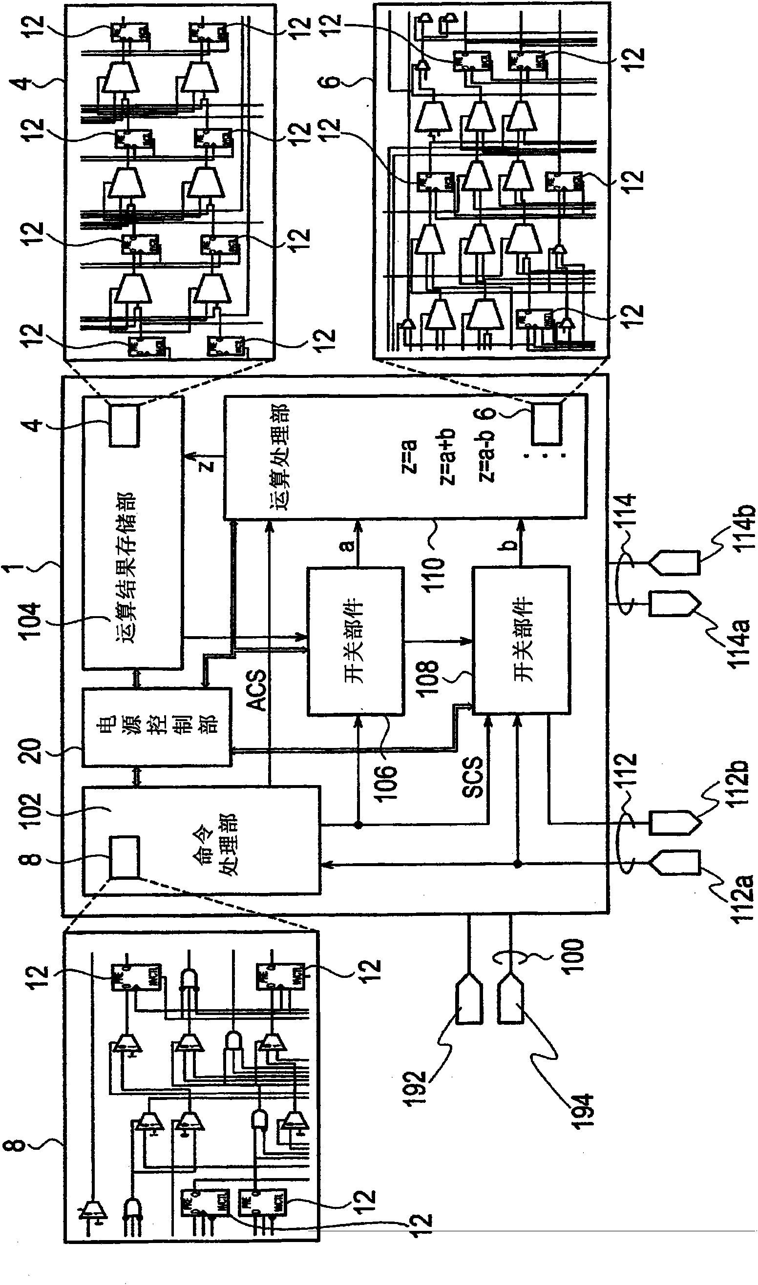
[0150] Such as figure 1 As shown, the non-volatile CPU 1 according to the first embodiment of the present invention includes: a command processing unit 102; a calculation processing unit 110, which is connected to the command processing unit 102 and receives the calculation control signal ACS from the command processing unit 102; a calculation result storage unit 104, which is connected to the calculation processing unit 110, and receives the calculation output signal z from the calculation processing unit 110; the switch part 106, which is connected to the calculation result storage unit 104 and the command processing unit 102, and supplies the output signal a to the calculation processing unit 110; The switch unit 108 is connected to the switch unit 106 and the command processing unit 102 , receives the switch control signal SCS from the command processing unit 102 , and supplies the output signal b to the arithmetic processing unit 110 .
[0151...
no. 2 approach
[0318] This implementation is in figure 1 In the illustrated nonvolatile CPU 1 , a nonvolatile memory gate 212 described below is applied instead of the nonvolatile memory gate 12 . Except for the point described below, the rest is the same as that of the first embodiment, and thus description thereof will be omitted.
[0319] (Example of configuration of nonvolatile memory gate 212)
[0320] Such as Figure 17 As shown, the nonvolatile memory gate 212 applicable to the nonvolatile memory gate built-in logic circuit of this embodiment includes: a volatile memory unit 224 including data holding circuits 133a, 133b, an inverter circuits 170 , 178 , and transfer gates 146 , 172 ; and a nonvolatile storage unit 218 having a ferroelectric capacitor 51 .
[0321] The data holding circuit 133b holds data by connecting the inverter circuits 136 and 138 in series in a loop at the time of data lock. The inverter circuit 136 is arranged on the main signal path, and the inverter circu...
no. 3 approach
[0385] This implementation is in figure 1 In the illustrated nonvolatile CPU 1 , a nonvolatile memory gate 412 described below is applied instead of the nonvolatile memory gate 12 . Except for the point described below, the rest is the same as that of the first embodiment, and thus description thereof will be omitted.
[0386] (Example of configuration of nonvolatile memory gate 412)
[0387] Such as Figure 22 As shown, the nonvolatile storage gate 412 applicable to the nonvolatile storage gate built-in logic circuit of this embodiment includes: a nonvolatile storage unit 418; a volatile storage unit 424, which receives data input Signal D, clock signal CK, output data output signal Q.
[0388] In the nonvolatile storage gate 412, the data interface control unit described in the above-mentioned embodiment is not shown as a circuit element, but the cell plate potential CP input to the nonvolatile storage unit 418 corresponds to the nonvolatile gate potential CP of the above...
PUM
 Abstract
Description
Claims
Application Information


