Liquid crystal display panel and manufacturing method thereof

Technology of a liquid crystal display panel and manufacturing method

Inactive Publication Date: 2011-02-02
BEIJING BOE OPTOELECTRONCIS TECH CO LTD
View PDF1 Cites 37 Cited by
  • Summary
  • Abstract
  • Description
  • Claims
  • Application Information

AI Technical Summary

Problems solved by technology

[0005] However, during the research process of the present invention, the inventors found that both of the above two solutions have certain defects: it is difficult to achieve a uniform distribution of glass spacers in the sealant, and it may cause two displays in places where glass spacers are densely packed. The gap between the substrates is large, while the sparse glass spacers lead to a small gap between the two display substrat

Method used


Image

  • Liquid crystal display panel and manufacturing method thereof
  • Liquid crystal display panel and manufacturing method thereof
  • Liquid crystal display panel and manufacturing method thereof

Examples


Embodiment 1

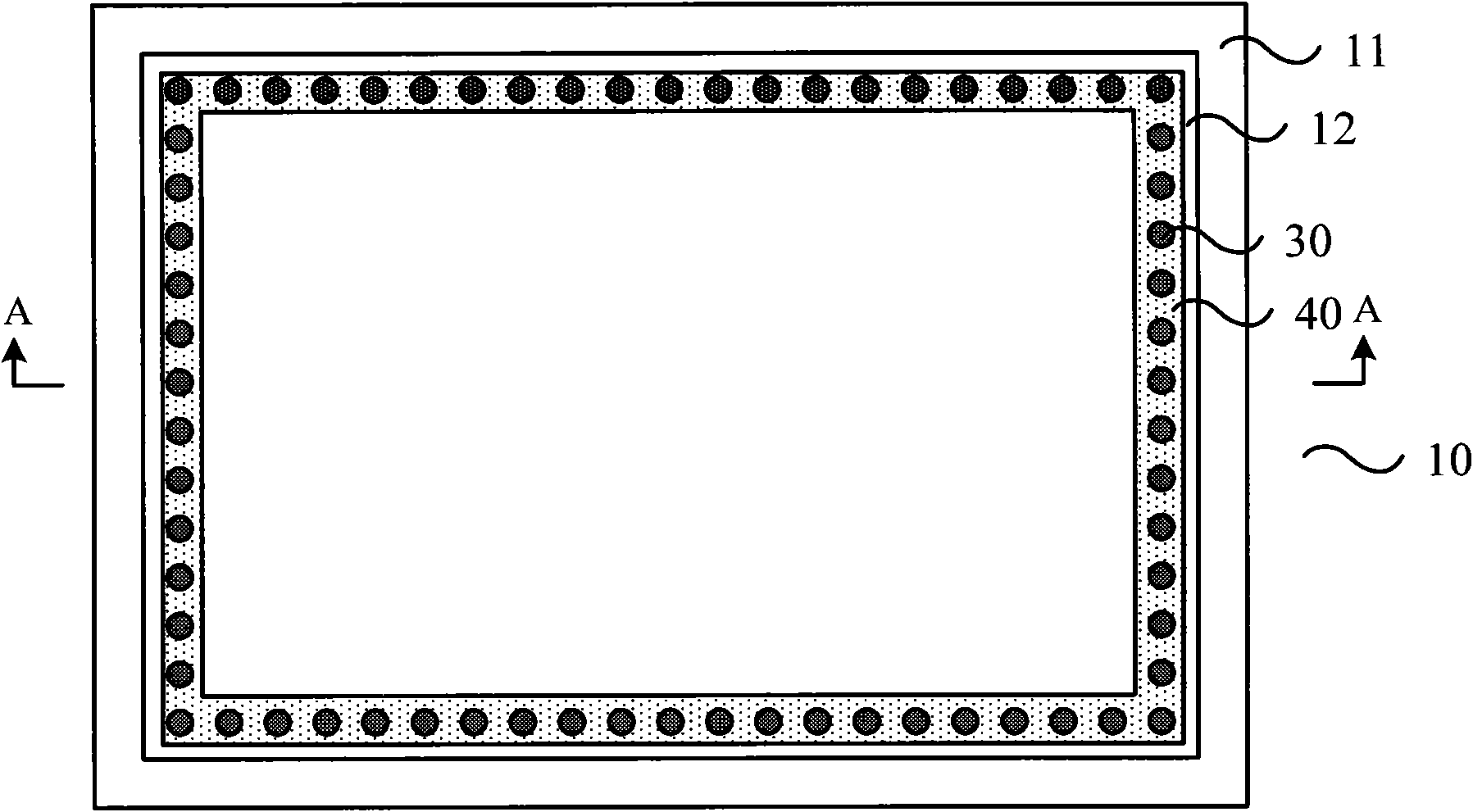
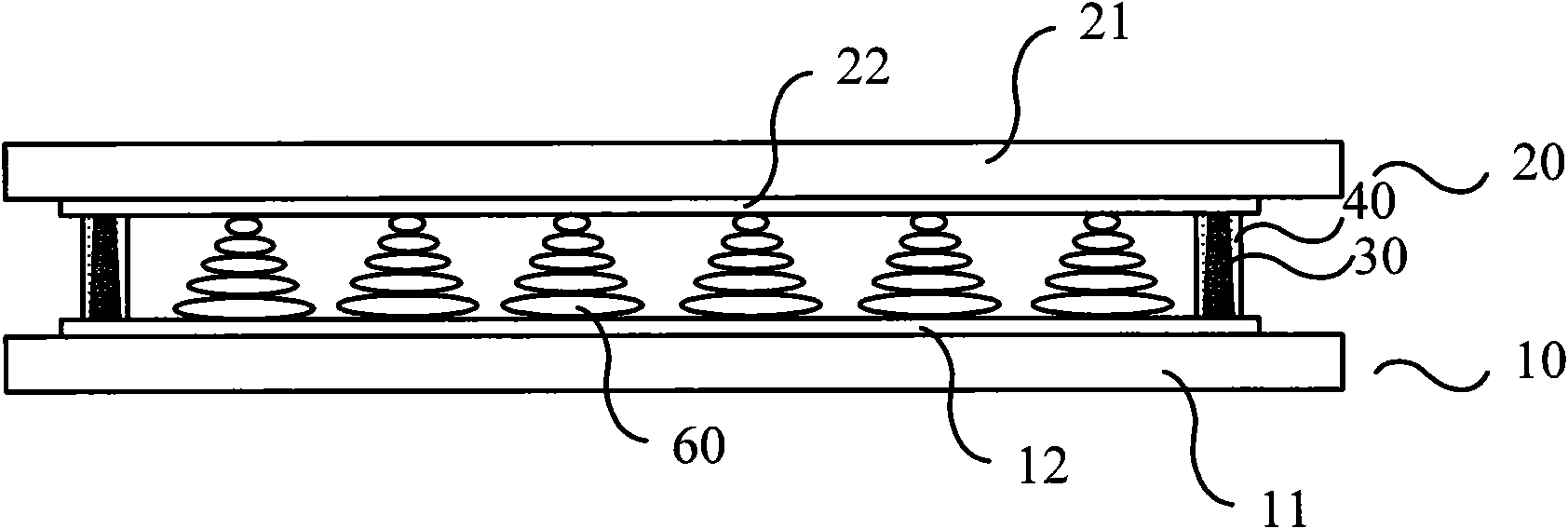
[0020] figure 1 It is a schematic plan view of the structure of the first display substrate in the liquid crystal display panel provided by Embodiment 1 of the present invention, figure 2 The liquid crystal display panel provided for Embodiment 1 of the present invention is figure 1 A schematic diagram of a side-view cross-sectional structure of the first display substrate cut along the line A-A. The liquid crystal display panel of this embodiment includes two display substrates arranged opposite to each other, that is, a first display substrate and a second display substrate. Generally, the first display substrate may be the array substrate 10 , and the second display substrate may be the color filter substrate 20 . The array substrate 10 includes a first base substrate 11 and an array functional film layer 12. The array functional film layer 12 can have various designs according to different display principles. For example, in the common thin film transistor (Thin Film T...

Embodiment 2

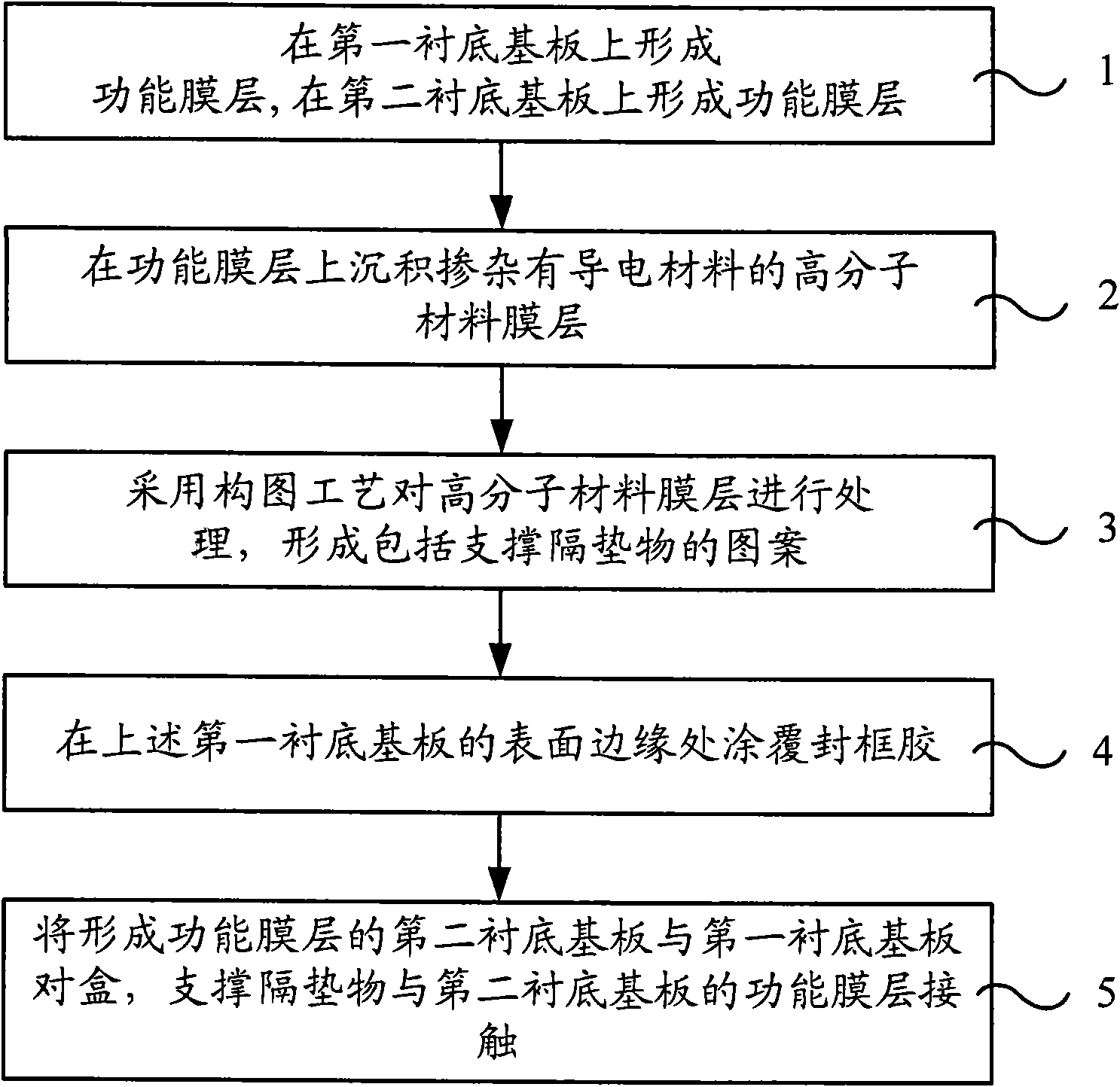
[0029] image 3 It is a flow chart of the manufacturing method of the liquid crystal display panel provided by the second embodiment of the present invention. The method is used to manufacture a liquid crystal display panel formed by pairing two display substrates. The two display substrates are usually an array substrate and a color filter substrate. The method specifically includes the following steps:

[0030] Step 1, forming a functional film layer on the first base substrate by multiple patterning processes, and forming a functional film layer on the second base substrate by patterning process;

[0031] Step 2. Form a polymer material film layer doped with a conductive material on the functional film layer of the first base substrate or the second base substrate. The polymer material film layer can be a polymer resin material, which can be obtained by deposition, etc. The process is formed on the surface of the functional film layer. It can cover the entire surface of t...


PUM


Abstract

The invention relates to a liquid crystal display (LCD) panel and a manufacturing method thereof. The liquid crystal display panel comprises two display substrates which are arranged opposite to each other, wherein a supporting spacer is formed at the edge of the surface of one display substrate by a composition process and contacted with the surface of the other display substrate; a frame sealing adhesive is also coated between the edges of the surfaces of the two display substrates; and a conducting material is doped in the frame sealing adhesive and/or the supporting spacer for electrically connecting the two display substrates. The manufacturing method comprises the following steps of: processing a high molecular material film layer by the composition process; forming a pattern comprising the supporting spacer at the edge of the surface of a functional film layer; coating the frame sealing adhesive; and folding up to ensure that the supporting spacer is in contact with the functional film layer of the second substrate. The supporting spacer is formed by the composition process, so that the position of the supporting spacer can be accurately controlled; and further, proper supporting force is provided for the liquid crystal display panel so as to keep the gap thickness between the liquid crystal display substrates and guarantee the display quality of the LCD.

Description

technical field [0001] Embodiments of the present invention relate to liquid crystal display technology, and in particular to a liquid crystal display panel and a manufacturing method thereof. Background technique [0002] A liquid crystal display panel is an important display component in a liquid crystal display (LCD for short), and the LCD is widely used in various electronic devices due to its small size, light weight, high image quality and long lifespan. [0003] The structure of a typical liquid crystal display panel includes two display substrates, each of which is provided with a corresponding functional film layer. Usually, the two display substrates are a color filter substrate and an array substrate respectively. The two display substrates are arranged in a pair of boxes, and liquid crystal molecules are filled in them. In order to encapsulate the liquid crystal molecules, a sealant is coated on the edge of the display substrate for sealing. The two display su...

Claims


Application Information

Patent Timeline
IPC IPC(8): G02F1/1333G02F1/1339
Inventor 张莹
Owner BEIJING BOE OPTOELECTRONCIS TECH CO LTD
Why Eureka
Try Eureka