Check patentability & draft patents in minutes with Patsnap Eureka AI!

P-type silicon-on-insulator transverse device for improving current density and preparation process thereof

A technology of silicon-on-insulator and lateral devices, which is applied in semiconductor/solid-state device manufacturing, semiconductor devices, electrical components, etc., to achieve the effects of saving production costs, increasing device current, and increasing current density

Active Publication Date: 2012-09-26
SOUTHEAST UNIV
View PDF0 Cites 0 Cited by
  • Summary
  • Abstract
  • Description
  • Claims
  • Application Information

AI Technical Summary

Problems solved by technology

This has also become a difficult problem in the design of power devices

Method used


Image

  • P-type silicon-on-insulator transverse device for improving current density and preparation process thereof
  • P-type silicon-on-insulator transverse device for improving current density and preparation process thereof
  • P-type silicon-on-insulator transverse device for improving current density and preparation process thereof

Examples


Embodiment Construction

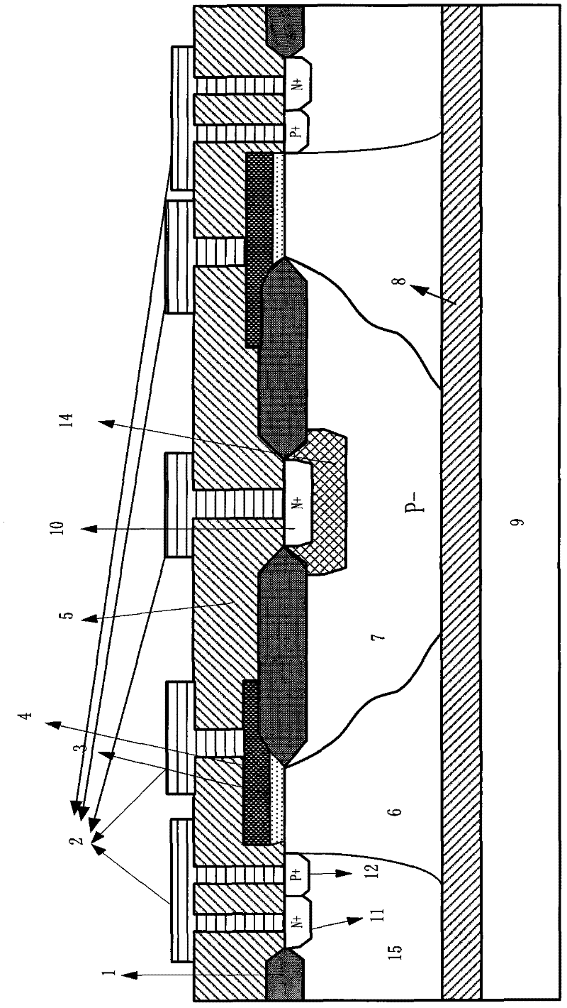
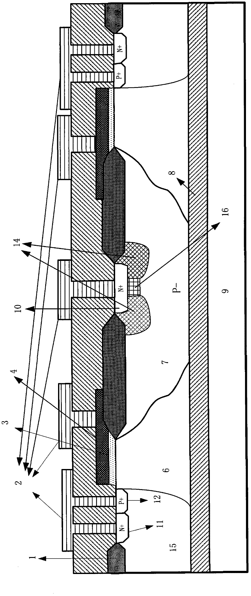
[0035] refer to figure 2 , a P-type silicon-on-insulator lateral device for increasing current density, comprising: an N-type semiconductor substrate 9 is provided with a buried oxide layer 8 on the semiconductor substrate 9, an N epitaxial layer 6 is provided on the buried oxide layer 8, and The N epitaxial layer is provided with a P-type drift region 7 and an N-type well region 15, and a P-type source region 12 and an N-type contact region 11 are arranged on the surface of the N-well region 15, and a P-type drift region 7 is provided on the P-type drift region 7. A buffer zone 14, an N-type drain region 10 is provided above the P-type buffer zone 14, and a gate oxide layer 3 is also provided on the surface of the N epitaxial layer 6, and the gate oxide layer 3 extends from the N epitaxial layer 6 to the P-type drift region 7. In the P-type source region 12 and the N-type contact region 11 on the surface of the N-type well region 15, a field oxide layer 1 is provided on the ...


PUM


Abstract

The invention relates to a P-type silicon-on-insulator (SOI) transverse device for improving current density, which comprises an N-type semiconductor substrate, wherein a buried oxygen layer is arranged on the semiconductor substrate, an N epitaxial layer is arranged on the buried oxygen layer, an N type drift region and an N well region are arranged on the N epitaxial layer, a P type source region and an N contact region are arranged on the surface of the N well region, a P type buffer region and a N type drain region are arranged on the P type drift region, a gate oxide layer is also arranged on the surface of the N epitaxial layer, a P type source region and an N type contact region are arranged on the surface of an N well, and a field oxide layer is arranged in a region beyond the N type drain region on the surface of the P type drift region. The P-type silicon-on-insulator transverse device is characterized in that the P type buffer region of the P-type silicon-on-insulator transverse device is an annular buffer region which diffuses inwards to form a P type buffer diffusion region. A method for preparing the P-type silicon-on-insulator transverse device comprises the following specific steps of: growing the N type epitaxial layer on SOI; preparing the N well and the P type drift region; preparing the annular P type buffer region; preparing filed oxygen and gate oxygen; preparing a polycrystal gate; preparing the source region and the drain region; preparing a through hole; and preparing a metal layer.

Description

Technical field: [0001] The invention relates to the field of power semiconductor devices, and more specifically relates to a P-type silicon-on-insulator lateral device with increased current density and a preparation process thereof, which is suitable for high-voltage and high-current applications. Background technique: [0002] With the increasing demand for modern life, the performance of power integrated circuits has attracted more and more attention. Among them, the ability of power integrated circuits to handle high voltage and high current has become one of the most important performance indicators. The factors that determine the ability of power integrated circuits to handle high voltage and high current are not only the circuit structure and design of the power integrated circuit itself, but also the manufacturing process adopted by the circuit. The current capability that a single device with the same area can pass is a measure of the performance and The key to cos...

Claims


Application Information

Patent Timeline
Patent Type & Authority Patents(China)
IPC IPC(8): H01L29/735H01L29/06H01L21/265H01L21/762H01L21/329
Inventor 孙伟锋钱钦松孙俊苏展时龙兴
Owner SOUTHEAST UNIV
Features
  • R&D
  • Intellectual Property
  • Life Sciences
  • Materials
  • Tech Scout
  • Unparalleled Data Quality
  • Higher Quality Content
  • 60% Fewer Hallucinations
Learn More