Check patentability & draft patents in minutes with Patsnap Eureka AI!

Bootstrap sampling switch circuit and bootstrap circuit

A bootstrap sampling switch and bootstrap circuit technology, applied in electronic switches, electrical components, pulse technology, etc., can solve the problems of increasing circuit complexity and achieve the effect of reducing complexity

Active Publication Date: 2012-07-04
昆山启达微电子有限公司
View PDF0 Cites 1 Cited by
  • Summary
  • Abstract
  • Description
  • Claims
  • Application Information

AI Technical Summary

Problems solved by technology

This additional clock voltage boost circuit increases the complexity of the circuit

Method used


Image

  • Bootstrap sampling switch circuit and bootstrap circuit
  • Bootstrap sampling switch circuit and bootstrap circuit
  • Bootstrap sampling switch circuit and bootstrap circuit

Examples


Embodiment Construction

[0047] In order to make the technical problems, technical solutions and advantages to be solved by the embodiments of the present invention clearer, the following will describe in detail with reference to the drawings and specific embodiments.

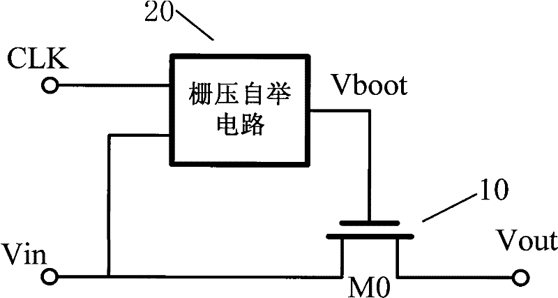
[0048] The present invention provides a bootstrap sampling switch circuit, comprising:

[0049] a bootstrap circuit and a ninth NMOS transistor M0;

[0050] The bootstrap circuit inputs the clock signal CLK and the signal Vin to be sampled, and outputs the first signal Vboot; the source of the ninth NMOS transistor M0 is connected to the signal Vin to be sampled, and the gate of the ninth NMOS transistor M0 is connected to the first signal Vboot , the drain of the ninth NMOS transistor M0 outputs the second signal Vout;

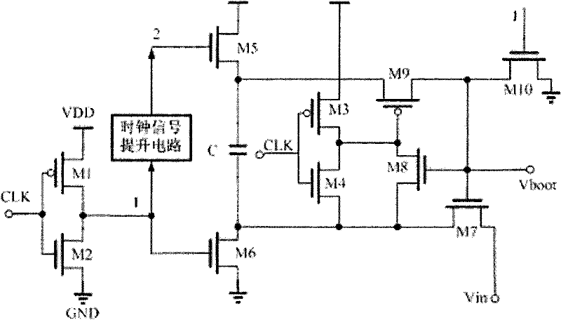
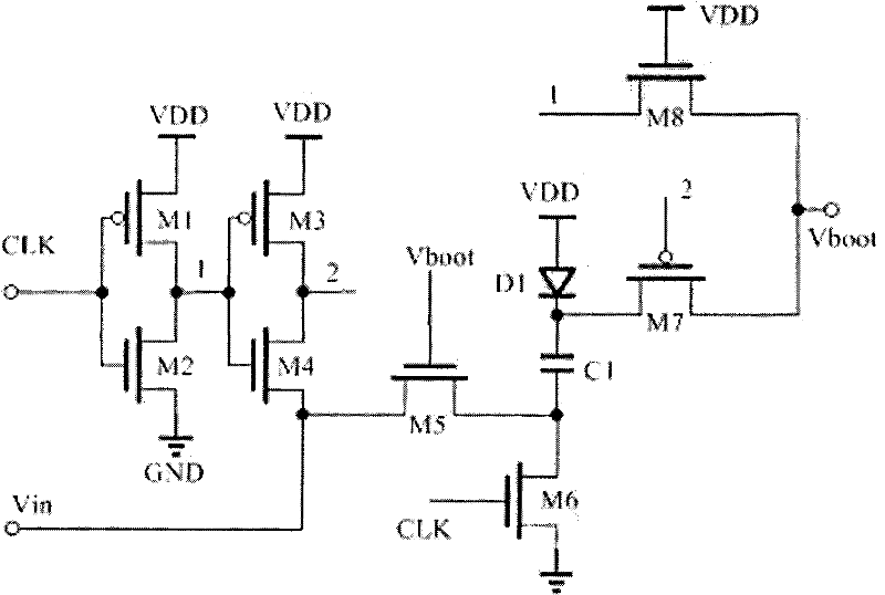
[0051] like image 3 As shown, the bootstrap circuit includes:

[0052]Diode, charging capacitor, inverter, third PMOS (P-channel metal oxide semiconductor FET, P-channel metal oxide semiconductor field effect tran...


PUM


Abstract

The invention provides a bootstrap sampling switch circuit and a bootstrap circuit. The bootstrap circuit comprises a diode D1, a charging capacitor C1, a phase inverter, a third P-channel metal oxide semiconductor (PMOS) tube M3, a fourth N-channel metal oxide semiconductor (NMOS) tube M4, a fifth NMOS tube M5, a sixth NMOS tube M6, a seventh PMOS tube M7 and an eighth NMOS tube M8, wherein the input end of the phase inverter is connected with a clock (CLK), while the output end is connected with the grid of the M3 and the grid of the M4; the source of the M3 is connected with a virtual device driver (VDD); the source of the M4 is connected with Vin; the drain of the M3 is connected with the drain of the M4; the source of the M5 is connected with the Vin; the grid of the M5 is connected with Vboot; the drain of the M5 is connected with the drain of the M6 and one plate of the capacitor; the grid of the M6 is connected with the CLK, while the source is connected with the ground (GND);the positive end of the D1 is connected with the VDD, while the negative end is connected with a second plate of the C1 and the source of the M7; the grid of the M7 is connected with the drain of theM3; the drain of the M7 and the source of the M8 are connected with the Vboot; and the grid of the M8 is connected with the VDD, while the drain is connected with the output end of the phase inverter.

Description

technical field [0001] The invention relates to the field of circuit design, in particular to a bootstrap sampling switch circuit and a bootstrap circuit. Background technique [0002] With the development of modern communication technology and signal processing technology, the demand for high-speed and high-precision semiconductor integrated circuits is increasing. In the field of analog processing, it is often necessary to convert an analog signal into a digital signal, and then perform further processing through a digital signal processing module. In the process of converting an analog signal to a digital signal, a sampling switch is often required to meet the performance requirements of the analog-to-digital converter. [0003] Based on the requirements for the performance of the sampling switch, a bootstrap sampling switch is often used. This technique is mainly used in sample and hold circuits. The structure of the bootstrap switch is as figure 1 As shown, the boot...

Claims


Application Information

Patent Timeline
Patent Type & Authority Patents(China)
IPC IPC(8): H03K17/687
Inventor 朱樟明孙园杰丁瑞雪刘帘曦李娅妮
Owner 昆山启达微电子有限公司
Features
  • R&D
  • Intellectual Property
  • Life Sciences
  • Materials
  • Tech Scout
  • Unparalleled Data Quality
  • Higher Quality Content
  • 60% Fewer Hallucinations
Learn More