Light emitting diode (LED) chip and LED wafer, and chip manufacturing method thereof

A LED chip and chip technology, applied in electrical components, electric solid devices, circuits, etc., can solve the problems of high packaging cost, LED heat dissipation technology and product complexity, and low packaging efficiency

Active Publication Date: 2011-03-09
秦彪
View PDF4 Cites 14 Cited by
  • Summary
  • Abstract
  • Description
  • Claims
  • Application Information

AI Technical Summary

Problems solved by technology

[0003] The heat transfer process in the LED chip is not complicated, but due to the fact that the knowledge of heat transfer and mature heat transfer technology, as well as other basic knowledge related to heat transfer, are not fully recognized by the LED industry, the current LED heat dissipation technology and The product is complicated and in its infancy
In addition, the disclosed LED chip packaging structure is developed along the previous low-power LED chip and traditional electronic chip packaging ideas, which not only makes the internal heat conduction and heat transfer resistance as high as the above, but also has low packaging efficiency and expensive packaging equipment. , the packaging cost is high, and it is difficult to realize the integrated packaging of optical modules

Method used


Image

  • Light emitting diode (LED) chip and LED wafer, and chip manufacturing method thereof
  • Light emitting diode (LED) chip and LED wafer, and chip manufacturing method thereof
  • Light emitting diode (LED) chip and LED wafer, and chip manufacturing method thereof

Examples


Embodiment Construction

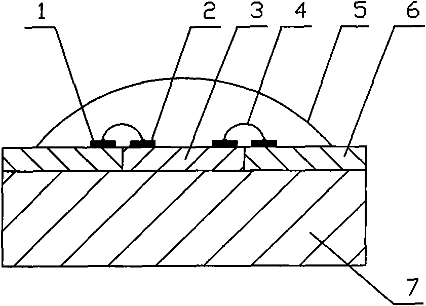
[0033] figure 1 In the shown LED chip of the present invention, the wafer 3 is embedded in the chip socket in the positioning piece 6, and the wafer 3 and the positioning piece 6 are attached to the A surface of the thermal diffusion member 7 together; Protective layer 5; the electrode pad 2 on the chip is close to the lead pad 1 on the positioning sheet, and the conduction connection between the two pads adopts an ultrasonic ball process, and the two ends of the wire 4 (gold wire or aluminum wire) are connected from the pad The surface stands up. Due to the thin wire diameter and low strength, the die-bonding protective layer 5 on the front of the chip should be set by dispensing. As shown in the figure, the thickness of the die-bonding protective layer 5 is uneven.

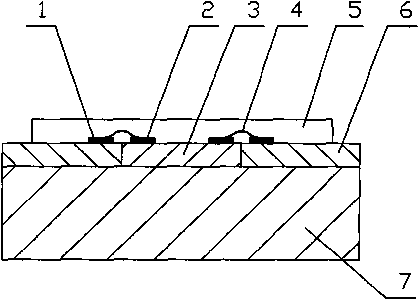
[0034] figure 2 As shown in the LED chip of the present invention, the two ends of the wire 4 are flatly attached to the two pads, and are welded by pressure welding. Since the wire lies flat, the strength is...


PUM


Abstract

Aiming at reducing thermal resistance, lowering cost and improving efficiency, the invention provides a light emitting diode (LED) chip encapsulation structure, an LED wafer structure and a chip manufacturing method. The wafer in the LED chip is embedded in a locating plate (6), and the wafer and the locating plate are attached to a thermal diffusion piece (7) through welding or adhesion. The thermal diffusion piece is made of copper, aluminum or copper-aluminum composite material, and the heat-flow density is effectively reduced after high heat-flow density on the wafer passes by the thermal diffusion piece, thus being beneficial to reducing the thermal resistance. A wire welding method, a solder welding method or a conductive adhesive is used to communicate the lead wire pad (1) on the locating plate with an electrode pad (2) on the front or side wall of the wafer. A solid wafer protective layer (5) is arranged on the front of the wafer, thus enabling the chip package production to be efficient and simple.

Description

technical field [0001] The invention belongs to the technical field of LEDs, and in particular relates to a packaging structure for heat conduction in LED chips and a chip structure for realizing low thermal resistance chips. technical background [0002] Heat dissipation has become a key issue in the development of high-power LEDs. LED heat dissipation can be divided into two major processes: internal heat conduction heat transfer process and external air convection heat transfer process. The thermal resistance of the internal heat conduction and heat transfer of the disclosed LED chip accounts for a very large proportion of the entire thermal resistance of the heat transfer, and the lowest thermal resistance of the current product must reach 6°C / W. If the thermal resistance of the insulating layer on the aluminum substrate is added, The minimum temperature should reach 10°C / W. [0003] The heat transfer process in the LED chip is not complicated, but due to the fact that...

Claims


Application Information

Patent Timeline
Patent Type & Authority Applications(China)
IPC IPC(8): H01L33/48H01L33/64H01L33/62H01L33/36H01L33/00
CPCH01L2224/45144H01L2224/48091H01L2924/181H01L2924/00014H01L2924/00012H01L2924/00
Inventor 秦彪
Owner 秦彪
Why Eureka
Try Eureka