Method for realizing integration of display image processing and timing control chip

A timing control chip and image processing technology, applied in static indicators, instruments, etc., can solve the problems of troublesome production process, large circuit board area, increase production cost, etc., to improve utilization rate, improve overall quality, and improve production. The effect of efficiency

Inactive Publication Date: 2011-03-30
TIANJIN SAMSUNG ELECTRONICS CO LTD
View PDF3 Cites 27 Cited by
  • Summary
  • Abstract
  • Description
  • Claims
  • Application Information

AI Technical Summary

Problems solved by technology

In this design scheme, the Main Board and X-Board are separated and independent, and the two circuit boards need to be connected through a special LVDS signal line; in terms of manufacturing, two separate printed circuit boards need to be made, and the two circuit boar

Method used


Image

  • Method for realizing integration of display image processing and timing control chip
  • Method for realizing integration of display image processing and timing control chip
  • Method for realizing integration of display image processing and timing control chip

Examples


Embodiment Construction

[0021] Below in conjunction with the accompanying drawings and preferred embodiments, the specific implementation, structure and features provided by the present invention are described in detail as follows:

[0022] In order to achieve the above object, the technical solution adopted by the present invention is: a method for realizing the integration of display image processing and timing control chip, and the implementation steps are as follows:

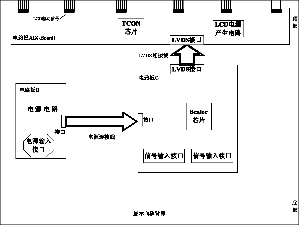
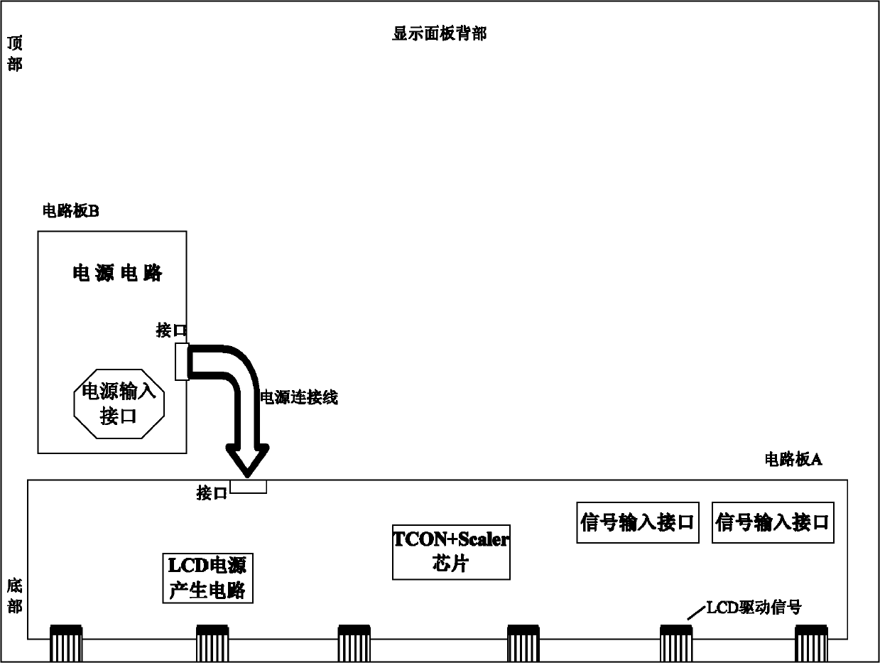
[0023] First, see figure 1 Specifically analyze the structural composition of the circuit of the existing display, the circuit of the display is mainly composed of three parts. Circuit board B mainly generates the power and backlight power required by the circuit board. The circuit board C is often called the main board (Main Board), and the most critical device is the Scaler, whose main task is to decode the external input signal into an LVDS signal output. The circuit board A (X-Board) is generally integrated with the display ...


PUM


Abstract

The invention relates to a method for realizing integration of a display image processing and timing control chip, which comprises the following implementation steps: (1) according to a signal flow of a display system, an image processing chip and a timing control chip are arranged in one chip; at the back end of image processing, a low voltage differential signaling (LVDS) signal output from a display control link is directly input into a data latch of a timing control (TCON) module; after data processing, the LVDS signal is output from a Mini-LVDS transmitting module; a source pole and gate pole control signal generating link is embedded into the image processing chip; and the output of the chip is a Mini-LVDS signal and corresponding control signals which are directly received and used by a liquid crystal display (LCD) panel; (2) a circuit board is in an integration structure, and except a power supply circuit board, other function modules are all concentrated on the circuit board; and (3) a power supply interface and an external signal input interface are arranged at the lower end of the back part of a display; and after the integration design of the circuit board is adopted, the liquid crystal panel needs to be flipped up and down. The invention has simplified structure, simple process and reliable performance.

Description

technical field [0001] The invention relates to a method for realizing the integration of display control chips, in particular to a method for realizing the integration of display image processing and timing control chips. Background technique [0002] With the rapid upgrading of the electronic market, LCD products have become the mainstream of consumption, the demand is increasing, and the output is also increasing. Therefore, it is urgent to improve production efficiency and improve production processes. [0003] The display function system is also applicable to the display system including Scaler (image processing, or called Display Controller, display control) and TCON (Timing Controller, timing control) functions. [0004] The currently developed display driver circuit has separate Scaler modules and TCON modules. Among them, the Scaler module is placed on the main board (Main Board), which mainly realizes the processing of various input signals, OSD (On-Screen Display...

Claims


Application Information

Patent Timeline
IPC IPC(8): G09G3/00G09G3/36
Inventor 陈军司骞
Owner TIANJIN SAMSUNG ELECTRONICS CO LTD
Why Eureka
Try Eureka