

Power bus structure used for multi-power supply chip
A power bus and multi-power technology, applied in the direction of circuits, electrical components, electric solid devices, etc., can solve the problems of increasing the chip area and affecting the electrostatic protection efficiency of the whole chip, and achieve the effect of reducing the area
- Summary
- Abstract
- Description
- Claims
- Application Information
AI Technical Summary
Problems solved by technology
Method used
Image

Examples
Embodiment approach
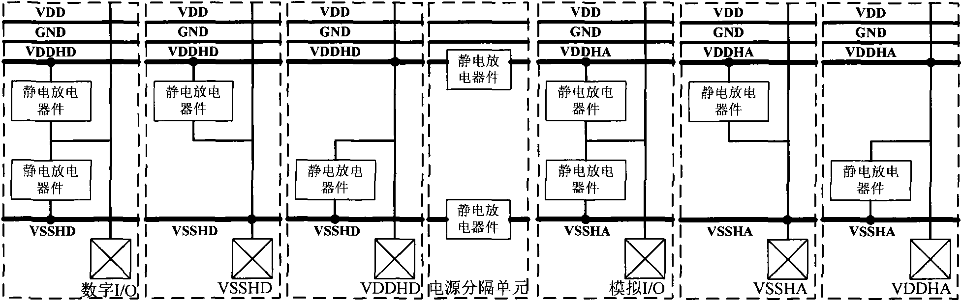
[0015] Based on this, an embodiment of the power bus structure of the present invention for a multi-power chip includes: a group of global power buses running through the entire chip and various groups of power supplies electrically connected to the global power bus, wherein,
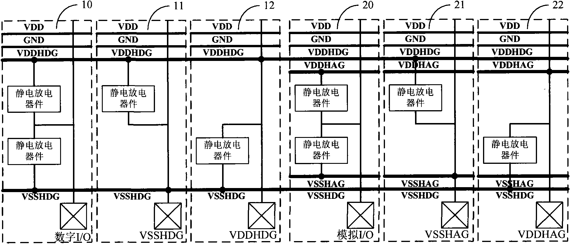
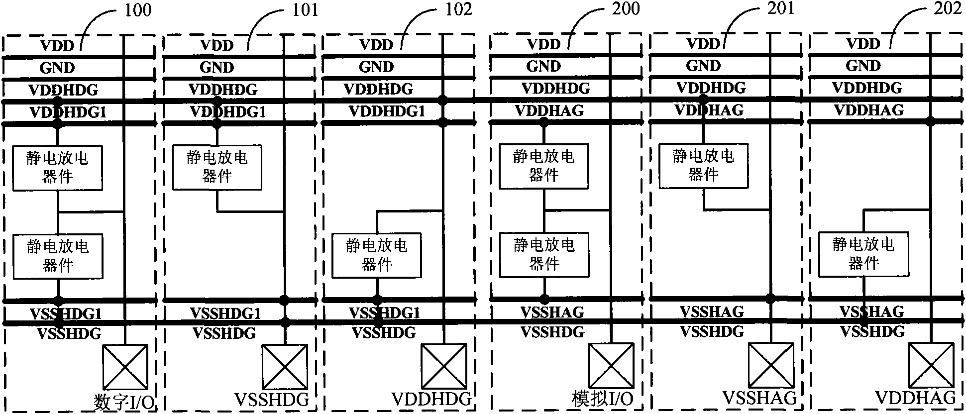
[0016] At least one group of power supplies in two adjacent groups of power supplies has a set of local power supply buses, and there are multiple power supply units in the power supply group, at least one of which has an electrostatic discharge device that separates the high-potential local power supply bus from the low-potential global power supply bus ; At least one other power supply unit has an electrostatic discharge device separating the low-potential local power bus from the high-potential global power bus.
[0017] In the above embodiments, by setting up a local power bus in at least one group of power supplies in two adjacent groups of power supplies, the power supply of this group is powered b...
PUM
 Abstract
Description
Claims
Application Information