Mother board of liquid crystal panel and manufacturing method thereof

A technology for liquid crystal panels and motherboards, applied in nonlinear optics, static indicators, optics, etc., can solve the problems of abnormal liquid crystal orientation, uneven cell thickness, affecting the picture quality of liquid crystal panels, and achieve uniform cell thickness and good flatness. sexual effect

Inactive Publication Date: 2011-04-13
BEIJING BOE OPTOELECTRONCIS TECH CO LTD
View PDF0 Cites 27 Cited by
  • Summary
  • Abstract
  • Description
  • Claims
  • Application Information

AI Technical Summary

Problems solved by technology

[0006] In the process of vacuum boxing of the color filter substrate and the array substrate, after the atmosphere is opened, since the air pressure inside and outside the main seal frame glue 4 is the same, spacers used to maintain the distance between the two substrates are different (eg image 3 As shown), therefore, the substrates inside and outside the main seal frame 4 receive different support forces, which can easily cause uneven thickness of a single panel in the peripheral area (inside and outside the main seal frame 4), resulting in abnormal orientation of the liquid crystal in this area and affecting the liquid crystal. panel picture quality

Method used


Image

  • Mother board of liquid crystal panel and manufacturing method thereof
  • Mother board of liquid crystal panel and manufacturing method thereof
  • Mother board of liquid crystal panel and manufacturing method thereof

Examples


Embodiment 1

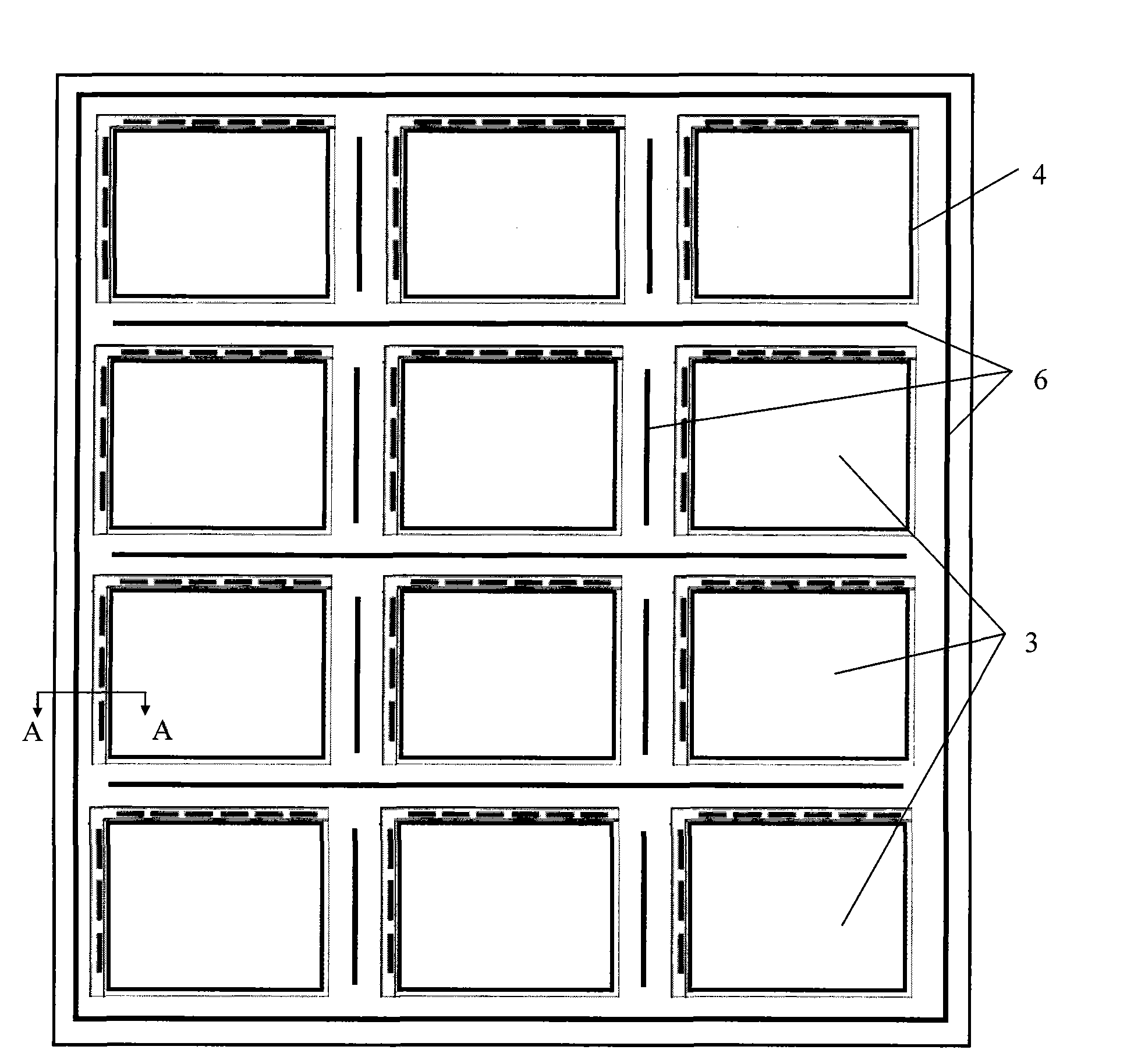
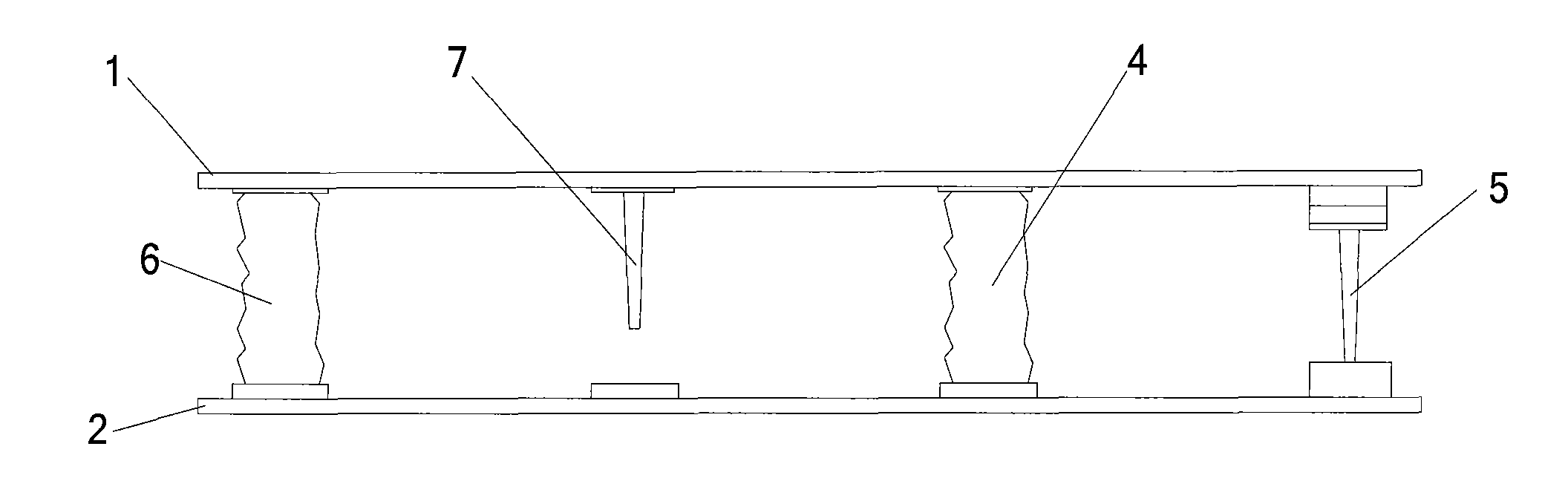
[0032] to combine Figure 4 and Figure 5 As shown, in the liquid crystal panel mother board provided in this embodiment, the auxiliary spacers formed between the main sealant 4 and the auxiliary sealant 6 are all columnar spacers 71, the bottom of which is deposited on the color On the film substrate 1 , the top end is supported on the array substrate 2 .

[0033]In addition, in this embodiment, the bottom area of ​​the auxiliary spacer 71 is greater than the bottom area of ​​the main spacer 5, and / or, the distribution density of the auxiliary spacer 71 is greater than the distribution density of the main spacer 5; Inside the area surrounded by the main sealant 4, that is, in the area of ​​a single panel, in addition to the main spacer 5 that maintains the distance between the two substrates, the liquid crystal filled therein can also play a certain role in maintaining the distance between the two substrates. Such a structure increases the contact area between the auxiliary...

Embodiment 2

[0036] combine Figure 4 and Figure 6 As shown, in the motherboard of the liquid crystal panel provided in this embodiment, the auxiliary spacer formed between the main sealant 4 and the auxiliary sealant 6 is a strip wall spacer 72, Its bottom is deposited on the color filter substrate 1 , and its top is supported on the array substrate 2 .

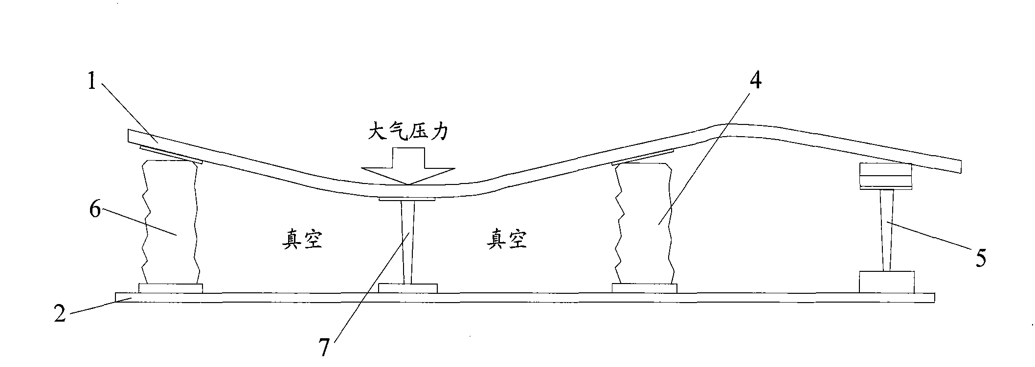
[0037] In some cases, it is necessary to set an opening on the auxiliary sealant 6 so that when the color filter substrate and the array substrate are boxed together, the atmosphere can enter the redundancy of the motherboard of the liquid crystal panel through the opening on the auxiliary sealant 6. In the remaining area, the air pressure inside and outside the substrate located in the redundant area is the same at this time, coupled with the supporting effect of the long wall-shaped spacer 72 arranged in the redundant area, the thickness of the box in the peripheral area of ​​a single panel remains uniform; and, The auxiliary spacer...

Embodiment 3

[0041] Corresponding to the above liquid crystal panel motherboard, in an embodiment of the present invention, a method for manufacturing a liquid crystal panel motherboard is also provided, including:

[0042] A spacer material is deposited on the substrate, followed by a mask exposure process in which the auxiliary spacer area is not exposed, the main spacer area is half-exposed, and the other areas are fully exposed, thereby forming a layer with a height difference on the substrate. Auxiliary spacers and main spacers.

[0043] Specifically, as Figure 7 As shown, the above-mentioned process of making a liquid crystal panel motherboard can be further refined as:

[0044] S1. Depositing a spacer material on the substrate.

[0045] A spacer material layer is formed on the color filter substrate or the array substrate by a CVD (Chemical Vapor Deposition, chemical vapor deposition) process, and the spacer material is photoresist.

[0046] Since the height of the main spacer i...


PUM

PropertyMeasurementUnit
thicknessaaaaaaaaaa
thicknessaaaaaaaaaa

Abstract

The embodiment of the invention discloses a mother board of a liquid crystal panel and a manufacturing method thereof, relating to the technical field of liquid crystal display. The invention can keep uniform box thickness between a color film base plate and an array base plate in the vacuum box folding process. The mother board of the liquid crystal panel comprises the color film base plate, the array base plate, a main frame sealing glue, an auxiliary frame sealing glue, a main partition substance and an auxiliary partition substance, wherein the array base plate is opposite to the color film base plate; the main frame sealing glue and the auxiliary frame sealing glue are formed between the color film base plate and the array base plate; liquid crystals are filled in an area encircled by the main frame sealing glue; the auxiliary partition substance and the main partition substance have different heights, and the distances between the color film base plate and the array base plate, which are kept after the auxiliary partition substance and the main partition substance respectively support against structural layers of the color film base plate and the array base plate, are equal. The mother board of the liquid crystal panel and the manufacturing method thereof are suitable for manufacturing any liquid crystal display device.

Description

technical field [0001] The invention relates to the field of liquid crystal display technology, in particular to a liquid crystal panel motherboard and a manufacturing method thereof. Background technique [0002] Thin Film Transistor-Liquid Crystal Display (TFT-LCD) has the characteristics of small size, low power consumption, no radiation, and relatively low manufacturing cost, and occupies a dominant position in the current flat panel display market. [0003] In the prior art, after the color filter substrate and the array substrate are box-aligned, in order to maintain the uniformity of the box thickness between the two-layer substrates, some materials are designed between the two-layer substrates for support, and these materials include the main spacer object, auxiliary spacer, main sealant and auxiliary sealant. [0004] figure 1 Shown is a schematic diagram of the structure of the color filter (Color filter, CF) substrate and the array (Array) substrate after boxing...

Claims


Application Information

Patent Timeline
Patent Type & Authority Applications(China)
IPC IPC(8): G02F1/133G02F1/1362G02F1/1368
CPCG02F2001/13396G02F1/1339G02F1/13396
Inventor 黄东升赵凯
Owner BEIJING BOE OPTOELECTRONCIS TECH CO LTD
Why Eureka
Try Eureka