

Chip fixing device and processing box with same for laser printer
A technology of laser printers and fixtures, applied in optics, electrical recording, instruments, etc., can solve problems such as low efficiency of integrated circuit chips
- Summary
- Abstract
- Description
- Claims
- Application Information
AI Technical Summary
Problems solved by technology
Method used
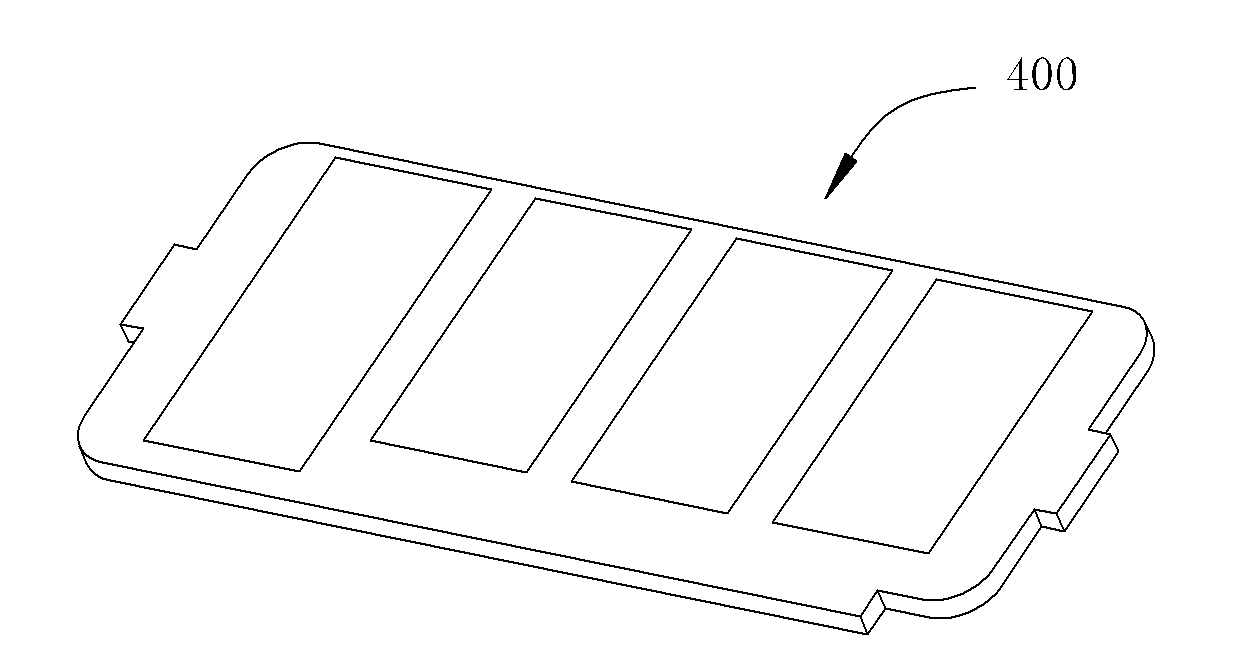
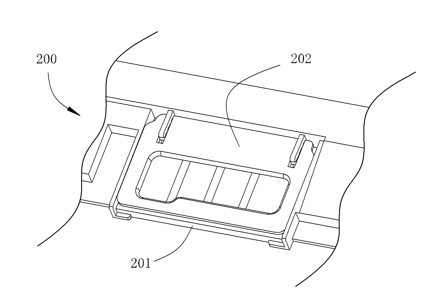
Image

Examples
Embodiment Construction
[0021] The chip fixing device of the present invention for installing integrated circuit chips and the process box for laser printers with the fixing device will be described in detail below in conjunction with the accompanying drawings.
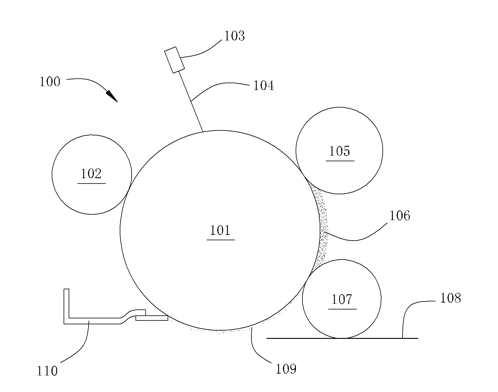
[0022] see Figure 1-9 , respectively show a perspective view and a cross-sectional view of the chip fixing device of the present invention and its related components under different viewing angles, and a schematic diagram of the basic structure of the process cartridge for a laser printer of the present invention with the chip fixing device.
[0023] Combined with the introduction of the background technology part of this paper, see figure 1 , 9 , 4, 6, the components of the process cartridge 100 for the laser printer of the present invention mainly include: a photosensitive drum 101 for forming an electrostatic latent image, a waste toner scraper 110 for removing residual toner on the surface of the photosensitive drum 101, and a photosen...
PUM
 Abstract
Description
Claims
Application Information