Liquid crystal display device
A liquid crystal display device, liquid crystal technology, applied in the direction of instruments, nonlinear optics, optics, etc., can solve the problems of disordered orientation, low brightness, dark lines, etc.
- Summary
- Abstract
- Description
- Claims
- Application Information
AI Technical Summary
Problems solved by technology
Method used
Image

Examples
Embodiment approach 1
[0109] A first embodiment of the liquid crystal display device of the present invention will be described below.
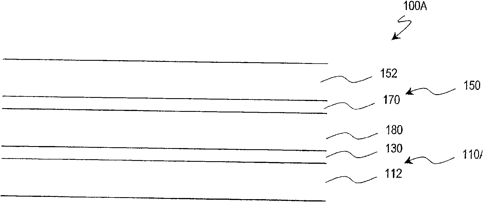
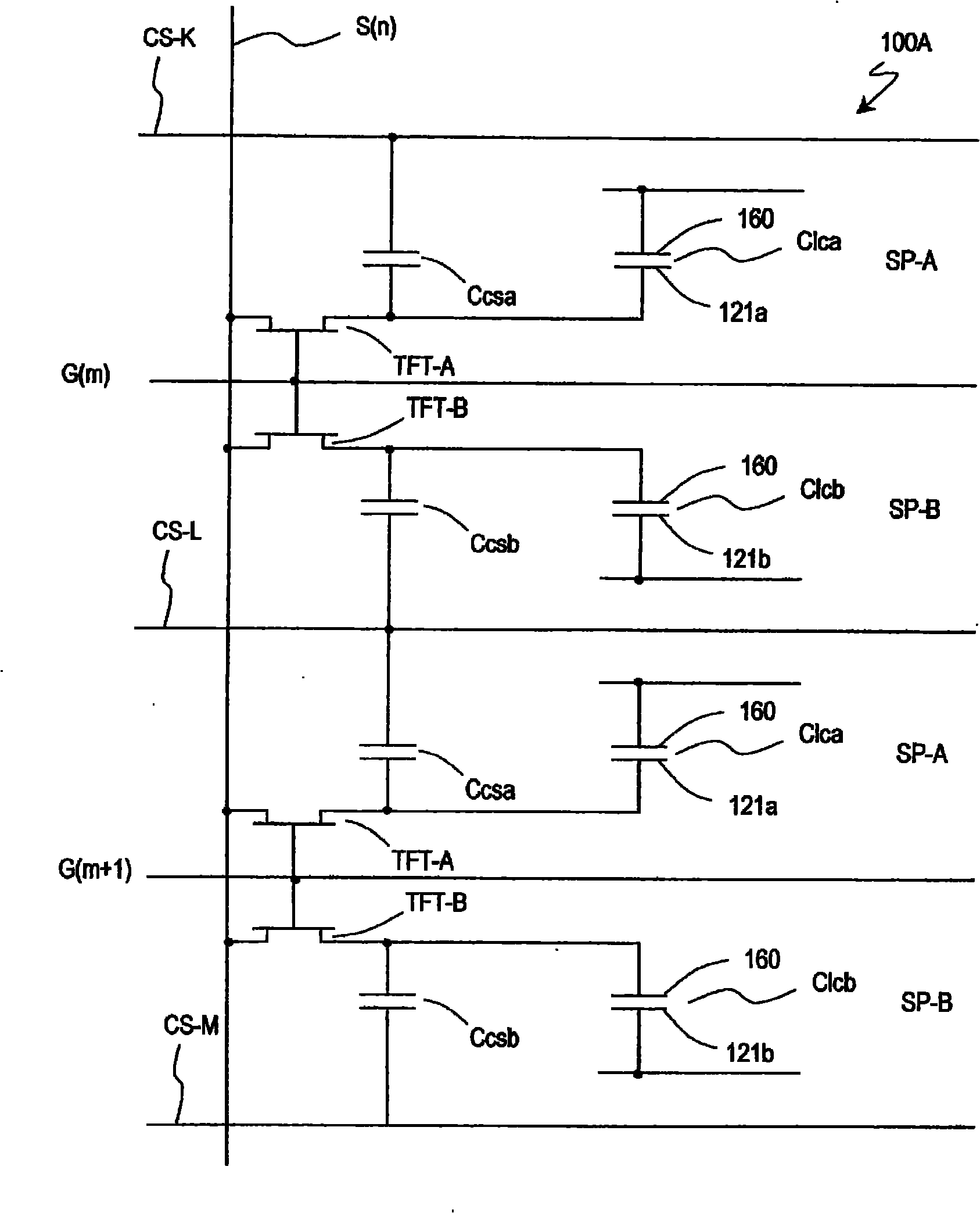
[0110] exist figure 1 A schematic diagram of a liquid crystal display device 100A of this embodiment is shown. The liquid crystal display device 100A includes an active matrix substrate 110A, a counter substrate 150 and a liquid crystal layer 180 . Active matrix substrate 110A has first alignment film 130 supported by insulating substrate 112 , and counter substrate 150 has second alignment film 170 supported by transparent insulating substrate 152 . The liquid crystal layer 180 is sandwiched between the first alignment film 130 of the active matrix substrate 110A and the second alignment film 170 of the counter substrate 150 . In addition, although in figure 1 Although not shown in the drawing, a plurality of wiring lines and pixel electrodes are provided between the insulating substrate 112 of the active matrix substrate 110A and the first alignment film 13...
Embodiment approach 2
[0193] A second embodiment of the liquid crystal display device of the present invention will be described below.
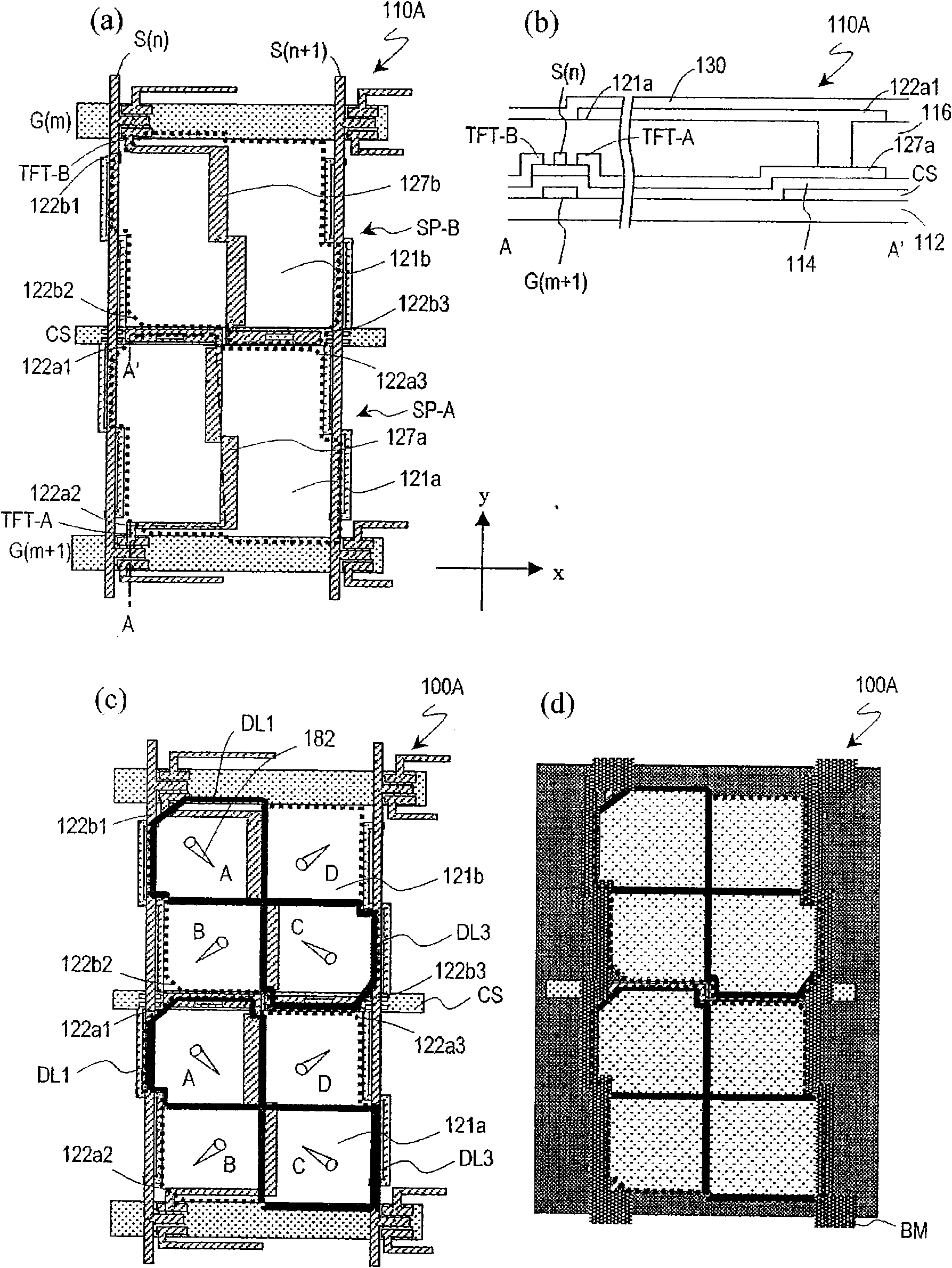
[0194] Figure 13(a) is a schematic plan view showing the structure of the active matrix substrate 110B in the liquid crystal display device 100B of the present embodiment, (b) is a schematic plan view showing dark lines generated in the liquid crystal display device 100B of the present embodiment, (c) is a schematic plan view of the liquid crystal display device 100B.
[0195] The liquid crystal display device 100B of this embodiment has the same configuration as the liquid crystal display device 100A, and redundant descriptions are omitted. In addition, the liquid crystal display device 100B is different from the liquid crystal display device 100A in that dark lines are generated in an inverted swastika shape.
[0196] exist Figure 13 (a) The second sub-pixel SP-B of the pixel in the mth row and the first sub-pixel SP-A of the pixel in the m+1th row are sho...
Embodiment approach 3
[0229] A third embodiment of the liquid crystal display device of the present invention will be described below.
[0230] Figure 22 (a) is a schematic plan view showing the structure of the active matrix substrate 110C of the liquid crystal display device 100C of the present embodiment, Figure 22 (b) is a schematic plan view showing dark lines generated in the liquid crystal display device 100C of the present embodiment. Figure 22 (c) and Figure 22 (d) is a schematic plan view of the liquid crystal display device 100C. Figure 22 (c) shows the positions of dark lines generated in the liquid crystal display device 100C and ribs or slits (openings) provided in the counter electrode. Figure 22 (d) shows the pattern of the black matrix BM.
[0231] The liquid crystal display device 100C of this embodiment has the same configuration as the liquid crystal display devices 100A and 100B, and redundant descriptions are omitted. In addition, the liquid crystal display device 1...
PUM
 Abstract
Description
Claims
Application Information
 - R&D
- Intellectual Property
- Life Sciences
- Materials
- Tech Scout
- Unparalleled Data Quality
- Higher Quality Content
- 60% Fewer Hallucinations
Browse by: Latest US Patents, China's latest patents, Technical Efficacy Thesaurus, Application Domain, Technology Topic, Popular Technical Reports.
© 2025 PatSnap. All rights reserved.Legal|Privacy policy|Modern Slavery Act Transparency Statement|Sitemap|About US| Contact US: help@patsnap.com