TFT-LCD array substrate and manufacture method thereof
An array substrate and gate line technology, applied in the field of TFT-LCD array substrate and its manufacturing, can solve the problems of over-etching or incomplete etching in the TFT channel area, so as to ensure product quality, increase storage capacitance, and increase yield Effect
- Summary
- Abstract
- Description
- Claims
- Application Information
AI Technical Summary
Problems solved by technology
Method used
Image

Examples
Embodiment Construction
[0066] The technical solutions of the present invention will be described in further detail below with reference to the accompanying drawings and embodiments.
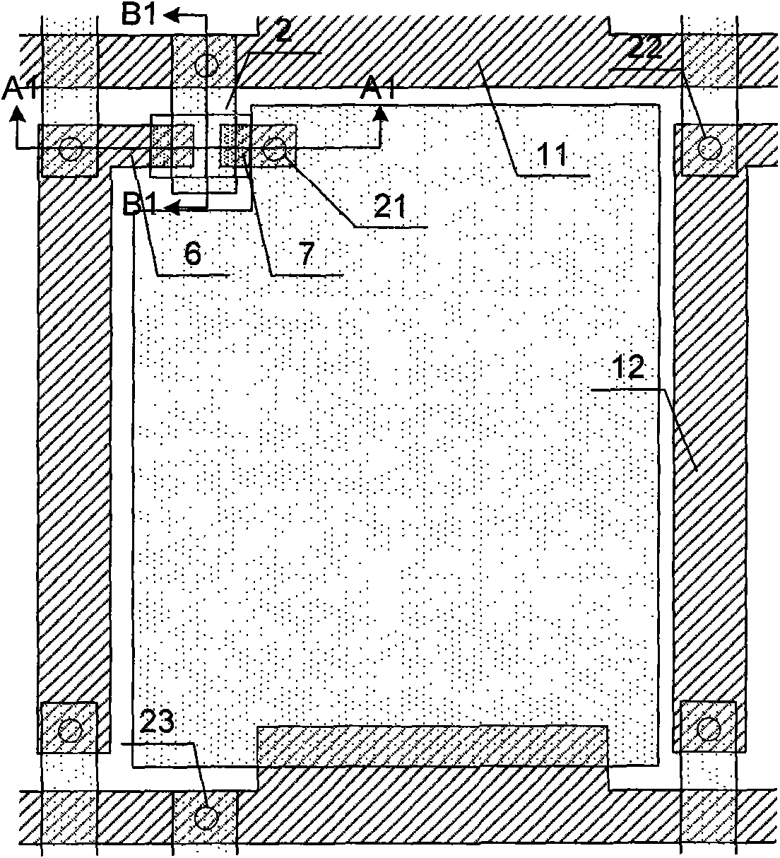
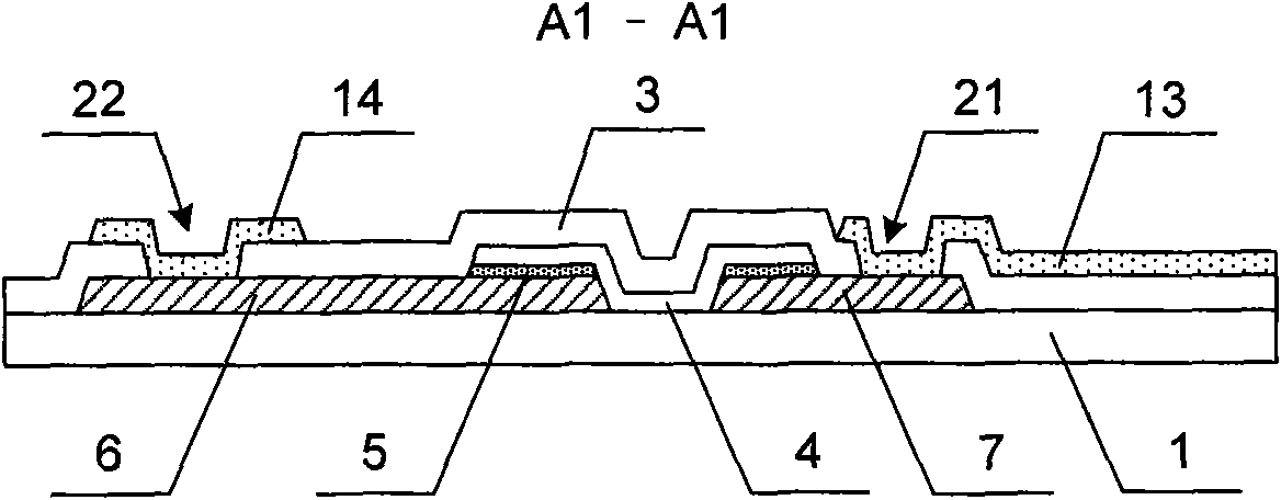
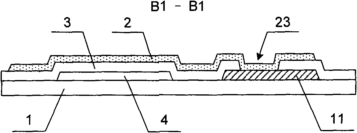
[0067] figure 1 It is a plan view of the first embodiment of the TFT-LCD array substrate of the present invention, reflecting the structure of a pixel unit, figure 2 for figure 1 The cross-sectional view of A1-A1 in the middle, image 3 for figure 1 Sectional view of B1-B1 direction in the middle. Such as Figure 1 ~ Figure 3 As shown, the main structure of the TFT-LCD array substrate in this embodiment includes gate lines 11, data lines 12, pixel electrodes 13 and thin film transistors, the gate lines 11 and data lines 12 perpendicular to each other define pixel regions, and the thin film transistors and pixel electrodes 13 is formed in the pixel area, the gate line 11 is used to provide the turn-on or turn-off signal to the thin film transistor, the data line 12 is used to provide the data signal to the pixel e...
PUM
 Abstract
Description
Claims
Application Information
 - R&D
- Intellectual Property
- Life Sciences
- Materials
- Tech Scout
- Unparalleled Data Quality
- Higher Quality Content
- 60% Fewer Hallucinations
Browse by: Latest US Patents, China's latest patents, Technical Efficacy Thesaurus, Application Domain, Technology Topic, Popular Technical Reports.
© 2025 PatSnap. All rights reserved.Legal|Privacy policy|Modern Slavery Act Transparency Statement|Sitemap|About US| Contact US: help@patsnap.com