TFT-LCD array substrate and method for manufacturing the same

The technology of an array substrate and manufacturing method is applied in the field of TFT-LCD array substrate and its manufacture, which can solve the problems of low aperture ratio, increase of drain electrode size, and small effective light-transmitting area, so as to increase aperture ratio, reduce brightness, and save The effect of manufacturing costs

Active Publication Date: 2011-04-20
BEIJING BOE OPTOELECTRONCIS TECH CO LTD
View PDF0 Cites 7 Cited by
  • Summary
  • Abstract
  • Description
  • Claims
  • Application Information

AI Technical Summary

Problems solved by technology

However, since this method increases the size of the drain electrode in the thin film transistor, there are technical defects such as small effective light-transmitting area and low aperture ratio.

Method used


Image

  • TFT-LCD array substrate and method for manufacturing the same
  • TFT-LCD array substrate and method for manufacturing the same
  • TFT-LCD array substrate and method for manufacturing the same

Examples


Embodiment Construction

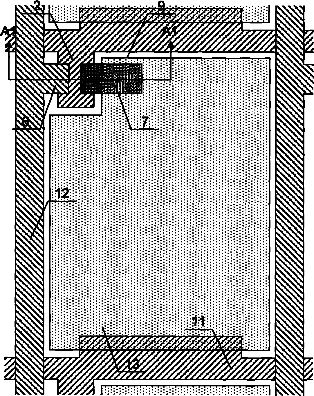
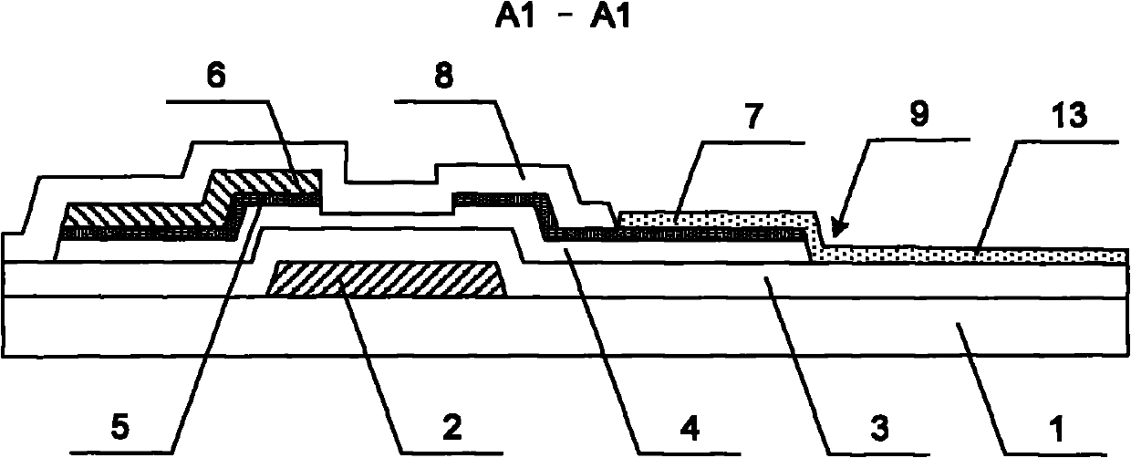
[0047] The technical solutions of the present invention will be described in further detail below with reference to the accompanying drawings and embodiments. The film thicknesses and area sizes and shapes of the various layers in the drawings do not reflect the true proportions of the TFT-LCD array substrate, but are only intended to schematically illustrate the contents of the present invention.

[0048] figure 1 It is a plan view of the TFT-LCD array substrate of the present invention, reflecting the structure of a pixel region, figure 2 for figure 1 Sectional view of A1-A1 in the middle. Such as figure 1 with figure 2As shown, the main structure of the TFT-LCD array substrate of the present invention includes gate lines 11, data lines 12, pixel electrodes 13 and thin film transistors formed on the substrate, and the gate lines 11 and data lines 12 perpendicular to each other define a matrix arrangement There are several pixel areas, each pixel area is formed with a ...


PUM


Abstract

The present invention relates to a TFT-LCD array substrate and a manufacturing method thereof. The TFT-LCD array substrate comprises gate lines and data lines, pixel electrodes and film transistors are formed in pixel areas defined by the gate lines and the data lines; the film transistor includes a gate electrode, a source electrode and a transparent drain electrode. The transparent drain electrode and the pixel electrode are positioned at the same layer, and they are formed in a same patterning process. The transparent drain electrode and the pixel electrodes are integrally structured. According to the invention, gate lines and gate electrodes are formed by a first patterning process, data lines and source electrodes are formed by a second patterning process, through holes in passivation layers are formed by a third patterning process, and transparent drain electrodes and pixel electrodes are formed by a fourth patterning process. Due to employment of the transparent electrode, light transmittance area of the pixel area is effectively increased, and aperture ratio is increased. The increasing aperture ratio can not only result in an increase in brightness, but also result in a decrease in brightness of backlight, therefore, energy consumption and manufacture cost can be saved.

Description

technical field [0001] The invention relates to a thin film transistor liquid crystal display and a manufacturing method thereof, in particular to a TFT-LCD array substrate and a manufacturing method thereof. Background technique [0002] Thin Film Transistor Liquid Crystal Display (TFT-LCD for short) has the characteristics of small size, low power consumption, and no radiation, and occupies a dominant position in the current flat panel display market. At present, five or four patterning processes are mainly used to manufacture TFT-LCD array substrates in the prior art. The five patterning processes mainly include: patterning of gate lines and gate electrodes, patterning of active layers, patterning of source / drain electrodes, patterning of via holes and patterning of pixel electrodes. The four-step patterning process is based on the five-step patterning process, and uses the half-tone or gray-tone mask technology to combine the active layer patterning and the source / drain...

Claims


Application Information

Patent Timeline
Patent Type & Authority Applications(China)
IPC IPC(8): G02F1/1362G02F1/1368H01L27/02H01L21/82H01L21/768
CPCG02F1/1368H01L29/458G02F1/13439H01L27/1214H01L27/12H01L27/124
Inventor 李伟李正勲
Owner BEIJING BOE OPTOELECTRONCIS TECH CO LTD
Why Eureka
Try Eureka