Opening and forming method thereof

A stage and change rate technology, applied in the field of openings and their formation in the passivation layer, can solve the problems of complex adjustment process and difficult realization, and achieve the effect of improving filling quality

Inactive Publication Date: 2011-04-20
SEMICON MFG INT (SHANGHAI) CORP +1
View PDF1 Cites 10 Cited by
  • Summary
  • Abstract
  • Description
  • Claims
  • Application Information

AI Technical Summary

Problems solved by technology

In this solution, the sidewall protection layer is formed or the high aspect ratio structure is etched mainly by adjusting the gas composition, which requires dynamic adjustment of the gas compos

Method used


Image

  • Opening and forming method thereof
  • Opening and forming method thereof
  • Opening and forming method thereof

Examples


Embodiment Construction

[0029] In order to make the above objects, features and advantages of the present invention more comprehensible, specific implementations of the present invention will be described in detail below in conjunction with the accompanying drawings.

[0030] In the following description, specific details are set forth in order to provide a thorough understanding of the present invention. However, the present invention can be implemented in many other ways than those described here, and those skilled in the art can make similar extensions without departing from the connotation of the present invention. Accordingly, the invention is not limited to the specific implementations disclosed below.

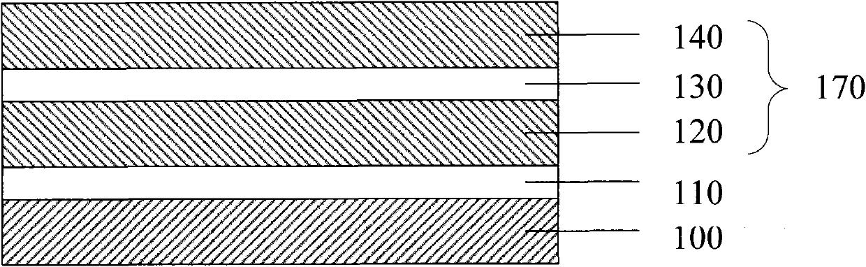
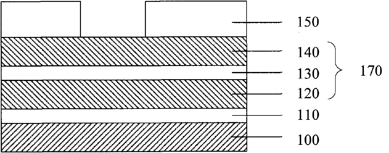
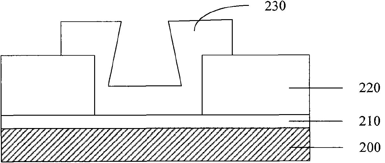
[0031] The method provided by the invention is not only applicable to the etching of the passivation layer in the 90nm process, but also applicable to the semiconductor processes of 65nm, 45nm and 32nm, and is also applicable to the etching of other dielectric layers that need to form special s...


PUM


Abstract

The invention discloses an opening and a forming method thereof. The forming method of the opening comprises the following steps of: dynamically adjusting fluoroform flow and bias power during main etching for forming the opening; and adjusting the amount of polymer produced during the etching, wherein the fluoroform flow is gradually increased and the bias power is gradually decreased. In the invention, the amount of the polymer produced during the etching can be adjusted by independently adjusting technological parameters of an etching menu and dynamically adjusting the fluoroform flow and the bias power during the main etching for forming the opening, so the appearance of the opening is influenced, the defect of increased square resistance of a filled metal layer caused by over-thick filling or bottom enlargement of the formed opening in the prior art are overcome, and the opening formed by the process contributes to improving the filling quality of the metal layer. In the process, related technological parameters in the etching menu are partially adjusted without addition of the complex process or obvious influence on the productivity and the production cost.

Description

technical field [0001] The invention relates to the field of semiconductor manufacturing, in particular to an opening in a passivation layer and a forming method thereof. Background technique [0002] With the rapid development of microelectronics technology, the size of CMOS (Complementary Metal Oxide Semiconductor) devices is also decreasing day by day. The current mainstream semiconductor process size has reached the order of 90nm and 65nm, and correspondingly, new requirements are constantly being put forward for the process technology. Wherein, after the passivation layer is etched in the back-end process (BEOL), it is necessary to fill the opening of the passivation layer with a metal layer to form a pad. When the line width of the device is large, there is no technical problem in filling the opening. With the continuous shrinking of the opening size, in order to reduce the sheet resistance (Rs) of the metal layer, the thickness of the metal layer needs to be increas...

Claims


Application Information

Patent Timeline
IPC IPC(8): H01L21/311H01L23/485
Inventor 张海洋孙武符雅丽
Owner SEMICON MFG INT (SHANGHAI) CORP
Why Eureka
Try Eureka