Capacitor and manufacturing method thereof

A technology of capacitors and electrodes, which is applied in the field of semiconductor devices, can solve problems such as complex processes, and achieve the effect of simple processes and improved capacitance

Inactive Publication Date: 2011-05-04
SEMICON MFG INT (SHANGHAI) CORP +1
View PDF3 Cites 2 Cited by
  • Summary
  • Abstract
  • Description
  • Claims
  • Application Information

AI Technical Summary

Problems solved by technology

[0007] From the above, the particles of the hemispherical particle silicon capacitor are arranged on the electrode, and in the manufacturing process of the hemispherical particle silicon capacitor, it is also necessary to feed oxygen to inhibit the growth of the particle, and the process is relatively complicated

Method used


Image

  • Capacitor and manufacturing method thereof
  • Capacitor and manufacturing method thereof
  • Capacitor and manufacturing method thereof

Examples


Embodiment Construction

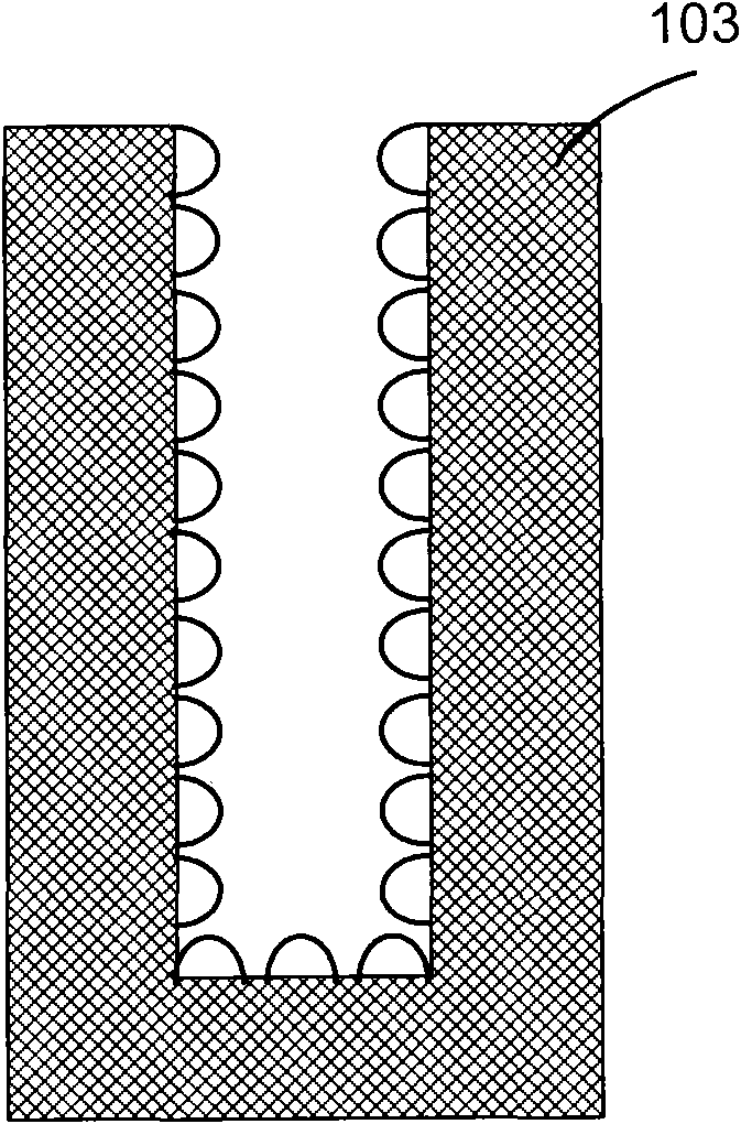
[0034] The present invention provides a capacitor, the capacitor includes a first electrode, a first dielectric layer on the first electrode, a silicon nanocrystal on the first dielectric layer, a silicon nanocrystal and the A second dielectric layer on the exposed portion of the first dielectric layer, a second electrode on the second dielectric layer. The silicon nanocrystals increase the interface area between the dielectric layer and the electrode, and when the capacitor is charged, more charges are attracted to the interface, thereby increasing the capacitance of the capacitor.

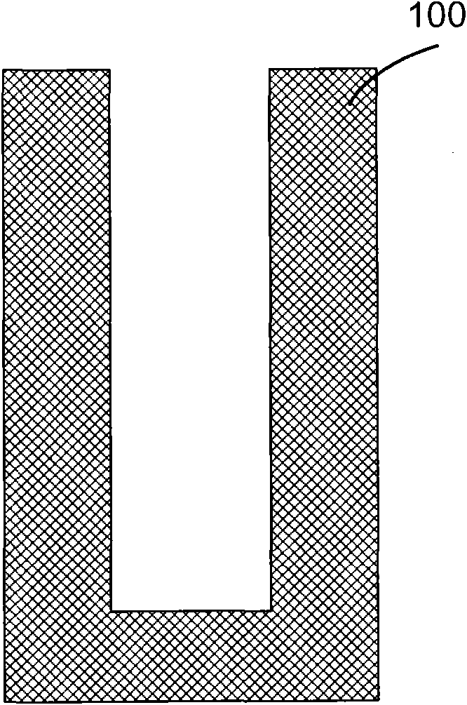
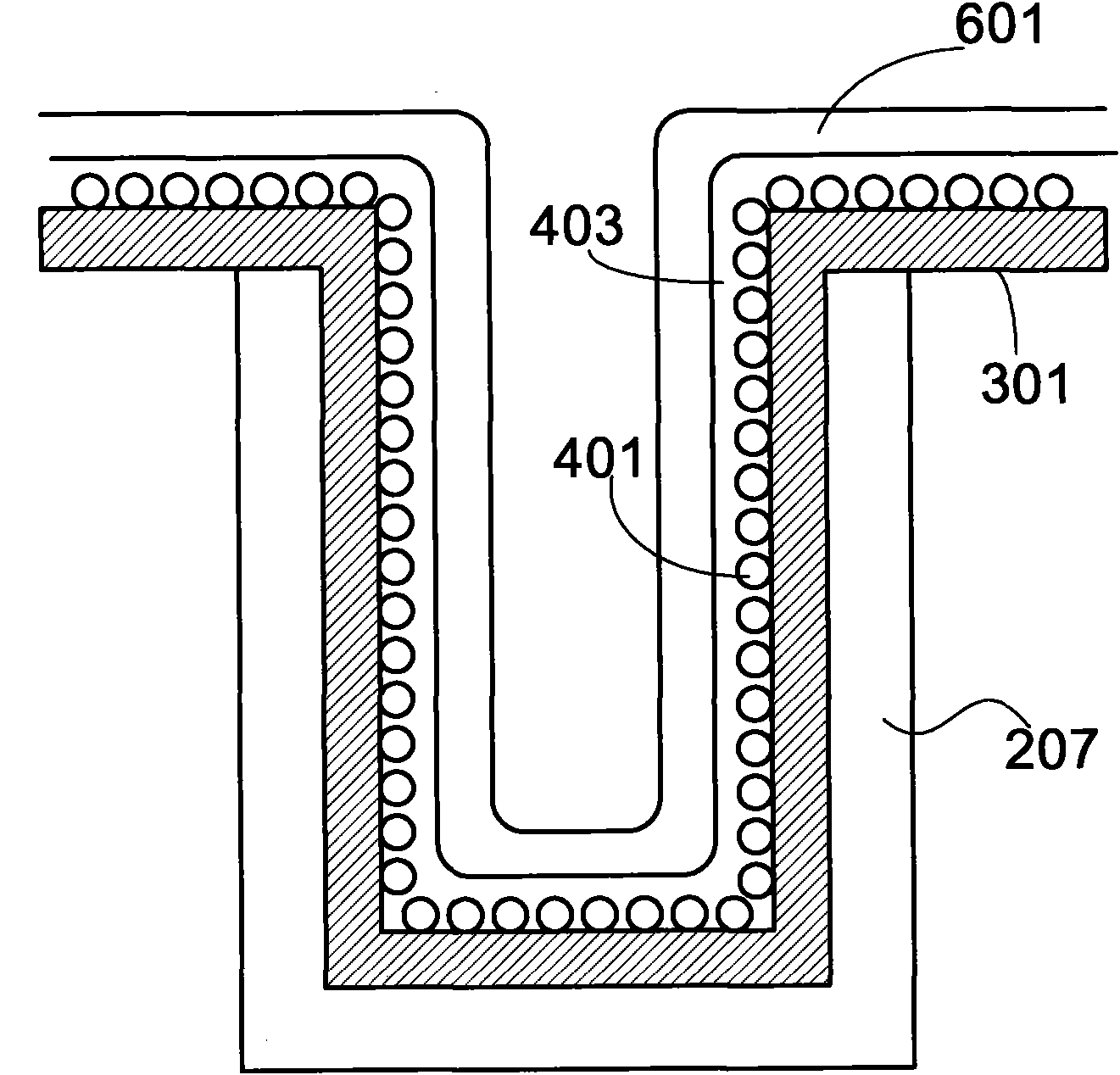
[0035] Specific examples reference figure 2 , figure 2 A schematic diagram of the structure of the capacitor according to the first embodiment of the present invention is given, and the capacitor includes a first electrode 207, and the first electrode is made of such as doped polysilicon, a compound of a conductive material, or a metal; the first electrode 207 has a first length and a first w...


PUM

PropertyMeasurementUnit
sizeaaaaaaaaaa
thicknessaaaaaaaaaa
sizeaaaaaaaaaa

Abstract

The invention relates to a capacitor and a manufacturing method thereof. The capacitor comprises a first electrode, a first dielectric layer positioned on the first electrode, a silicon nanocrystal positioned on the first dielectric layer, a second dielectric layer positioned on the silicon nanocrystal and the first dielectric layer which is not covered by the silicon nanocrystal and a second electrode positioned on the second dielectric layer. The manufacturing process of the capacitor is based on the traditional technology and is simple. By using the silicon nanocrystal, the invention increases the capacitance of the capacitor.

Description

technical field [0001] The invention relates to the field of semiconductor devices, in particular to a capacitor and a manufacturing method thereof. Background technique [0002] Integrated circuits have grown from a handful of interconnected devices fabricated on a single chip to millions of devices. The performance and complexity of traditional integrated circuits have far exceeded imagination. To achieve increases in the complexity and density of integrated circuits, feature sizes have become smaller and smaller with each generation of integrated circuits. [0003] Increases in circuit density not only increase the complexity and performance of integrated circuits, but also provide customers with cheaper electronic devices. A set of integrated circuits or chip-making equipment can cost millions, or even billions of dollars. Each set of manufacturing equipment has a certain wafer output, and there will be a certain number of integrated circuits on each wafer. Thus, by ...

Claims


Application Information

Patent Timeline
Patent Type & Authority Applications(China)
IPC IPC(8): H01L29/92H01L21/02H01L21/205
CPCB82Y10/00H01L28/84H10B12/033
Inventor 三重野文健
Owner SEMICON MFG INT (SHANGHAI) CORP
Why Eureka
Try Eureka