Stack type package structure and manufacture method thereof

A technology of packaging structure and manufacturing method, applied in semiconductor/solid-state device manufacturing, semiconductor/solid-state device parts, semiconductor devices, etc., can solve problems such as sticking

Active Publication Date: 2011-05-11
ADVANCED SEMICON ENG INC
View PDF8 Cites 3 Cited by
  • Summary
  • Abstract
  • Description
  • Claims
  • Application Information

AI Technical Summary

Problems solved by technology

Furthermore, the upper die and the lower die are currently ultra-thin, so how to absorb these thin dies and carry out flip-chip stacking of thin dies is a major challenge
Fin

Method used


Image

  • Stack type package structure and manufacture method thereof
  • Stack type package structure and manufacture method thereof
  • Stack type package structure and manufacture method thereof

Examples


Embodiment Construction

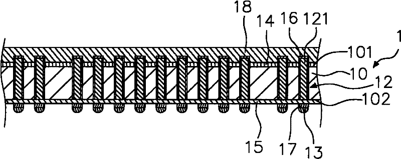
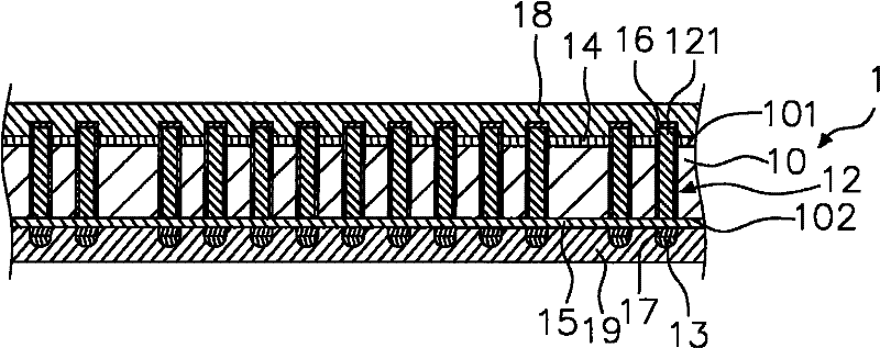
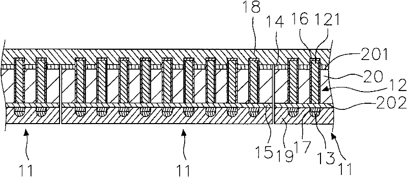
[0011] refer to Figures 1 to 14 , is a schematic diagram showing the first embodiment of the manufacturing method of the stacked package structure of the present invention. refer to figure 1 , providing a first wafer 1 and a tape (Tape) 18 . The first wafer 1 includes a first wafer body 10 , a plurality of first through silicon vias (TSVs) 12 and a plurality of first bumps 13 . The first wafer body 10 includes a first surface 101 and a second surface 102 . The first connecting pillars 12 pass through the first wafer body 10 , and one ends 121 of the first connecting pillars 12 protrude from the first surface 101 . The first bumps 13 are adjacent to the second surface 102 and electrically connected to the first vias 12. In this embodiment, the first bumps 13 are stacks of copper pillars and solders. structure. In other embodiments, the first bumps 13 may only be copper pillars or solder. The adhesive tape 18 is adjacent to the first surface 101 to cover and protect the e...


PUM


Abstract

The invention relates to a stack type package structure and a manufacture method thereof. The method comprises the steps of: forming and curing a first protective layer for covering a first convex block of a first wafer; cutting the first wafer to form a plurality of first crystal particles; forming a second protective layer for covering a second convex block of a second wafer; absorbing the first crystal particles by using a joint through the first protective layer, jointing the first crystal particles on the second wafer; removing the joint, removing part of the first protective layer; cutting the second wafer to form a plurality of second crystals; forming a third protective layer on a base plate; and jointing the first crystal particles and the second crystal particles on the base plate. Therefore, the first protective layer can protect the first convex block, and the first protective layer has the function of increasing the thickness and flattening so as to be beneficial to the absorption of the first crystal particles.

Description

technical field [0001] The present invention relates to a packaging structure and a manufacturing method thereof, in particular, to a stacked packaging structure and a manufacturing method thereof. Background technique [0002] Stacked packaging structure is a three-dimensional packaging structure formed by stacking two dies (lower die and upper die) on a substrate, in which the lower die located below will have several through silicon vias (TSV) structure, these connecting pillars protrude from one surface of the lower die, and the other surface of the lower die has several bump structures. Therefore, the following problems may be encountered in the process of manufacturing the stacked package structure. [0003] Firstly, during the process, the via structures or the bump structures will be damaged when the lower die is adsorbed by the bonding head. Furthermore, currently the upper die and the lower die are ultra-thin, so how to absorb these thin die and perform flip-chip...

Claims


Application Information

Patent Timeline
IPC IPC(8): H01L21/98H01L25/065H01L23/00H01L23/28H01L23/31
CPCH01L2224/05569H01L2224/83005H01L2224/75301H01L2224/83002H01L23/3121H01L23/3128H01L24/05H01L24/06H01L21/6836H01L24/73H01L24/75H01L24/81H01L24/83H01L24/97H01L25/0657H01L25/50H01L2221/68327H01L2224/0401H01L2224/05009H01L2224/0557H01L2224/06181H01L2224/131H01L2224/13147H01L2224/16145H01L2224/16225H01L2224/2919H01L2224/73104H01L2224/7565H01L2224/81002H01L2224/81005H01L2224/97H01L2225/06517H01L2924/00014H01L2924/01079H01L2924/15311H01L2224/05568H01L2224/11009H01L2225/06513H01L2225/06541H01L2225/06544H01L2225/06548H01L2224/94H01L2224/81007H01L2224/83007H01L21/76898H01L2224/11H01L2224/13H01L2224/16H01L2924/014H01L2224/81H01L2224/05552H01L2924/00012H01L2924/00
Inventor 陈仁川张惠珊赖宥丞
Owner ADVANCED SEMICON ENG INC
Why Eureka
Try Eureka