Semiconductor devices and methods
A technology of semiconductors and devices, applied to semiconductor devices and their fields
- Summary
- Abstract
- Description
- Claims
- Application Information
AI Technical Summary
Problems solved by technology
Method used
Image


Examples
Embodiment Construction
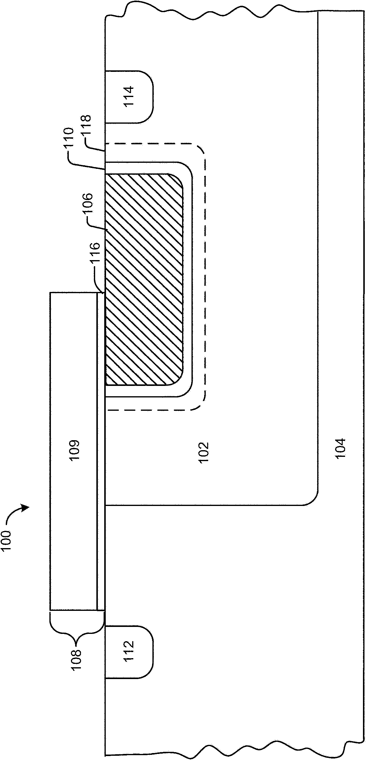
[0012] Described herein are structures of semiconductor devices, such as LDMOS devices, and systems and methods of forming semiconductor devices, such as LDMOS devices.
[0013] According to one embodiment, the LDMOS device includes: a first doped region (for example, a well) in a semiconductor substrate, a trench isolation region, an area covering at least a part of the first doped region (for example, a well) and the trench isolation region. At least a portion of the gate, a second doped region between the first doped region and the trench isolation region. The second doped region forms a p-n junction with the first doped region having a space charge region between the first doped region and the second doped region.
[0014] According to another embodiment, the LDMOS device includes: a first doped region, a trench isolation region, and a second doped region at least partially surrounding the trench isolation region in the first doped region. The second doped region has the ...
PUM
 Abstract
Description
Claims
Application Information