Check patentability & draft patents in minutes with Patsnap Eureka AI!

Method and device for plugging hole by using piston during printed circuit board manufacture

A technology for printed circuit boards and plug holes, which is applied in the direction of printed circuit manufacturing, printed circuits, and the formation of electrical connections of printed components. sunken effect

Inactive Publication Date: 2011-05-11
HUNAN GLOBAL ELECTRONICS TECH
View PDF0 Cites 13 Cited by
  • Summary
  • Abstract
  • Description
  • Claims
  • Application Information

AI Technical Summary

Problems solved by technology

[0005] The technical problem to be solved by the present invention is to provide a special plugging device for the problems of hole depression and air bubbles in the plugging technology of making printed circuit boards.

Method used


Image

  • Method and device for plugging hole by using piston during printed circuit board manufacture
  • Method and device for plugging hole by using piston during printed circuit board manufacture

Examples


Embodiment Construction

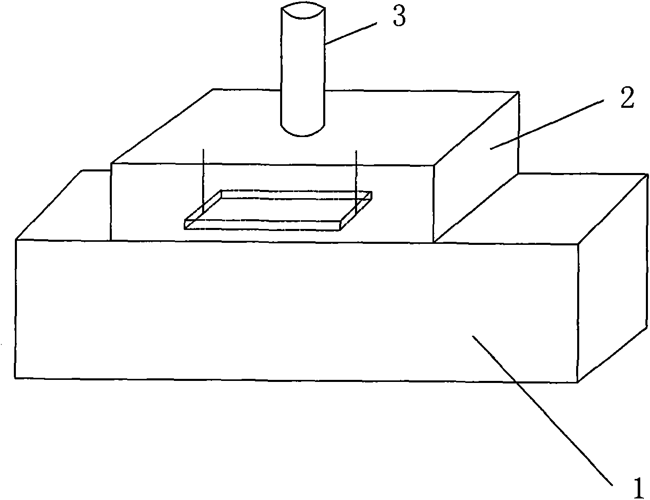
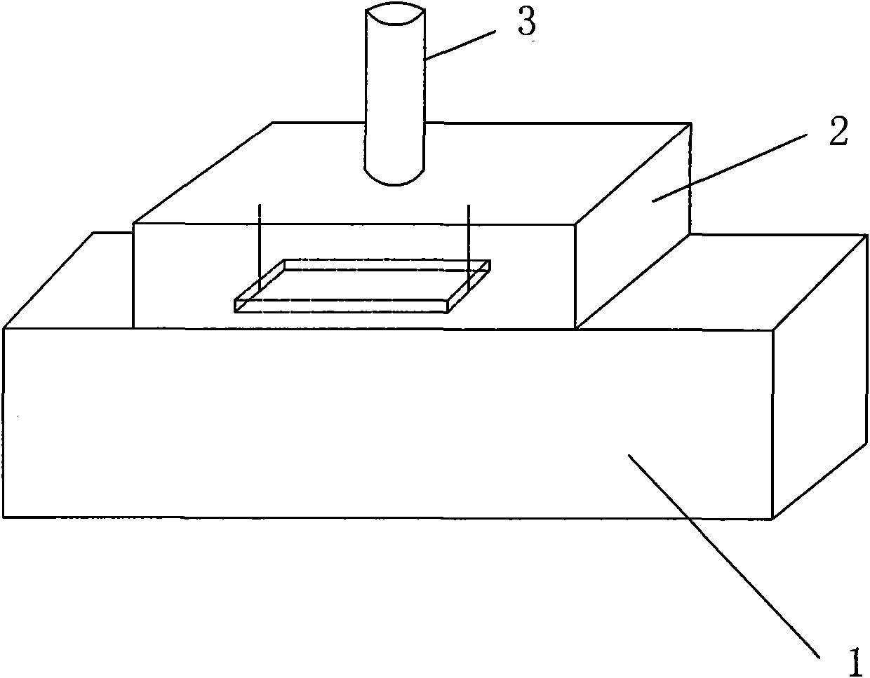
[0016] see figure 1 , the device includes a pallet 1 for placing printed circuit boards, a cavity 2 is formed on the top of the pallet 1, and the lower part of the cavity 2 is open, and a screen or a prepreg or an aluminum sheet is placed at the opening, and then placed on their A large amount of ink, resin or copper paste is preset on the top, a piston 3 is installed on the top of the cavity 2, and the surroundings of the cavity 2 are sealed. During the production process, the piston 3 of the device compresses the air in the closed cavity 2 in the through hole or blind hole of the circuit board, and then the air compresses the ink on the aluminum sheet, mesh plate or prepreg sheet covered on the circuit board. , resin or copper paste to apply pressure and fill ink, resin or copper paste into the via hole or blind hole, so that the via hole or blind hole of the circuit board is completely filled with ink, resin or copper paste, effectively preventing air bubbles And dents and...


PUM


Abstract

The invention relates to a method and a device for manufacturing a printed circuit board, in particular to a method and a device for plugging a via hole and a blind hole of the printed circuit board. In the invention, a network board, a prepreg or an aluminum sheet is placed in an opening at the lower part of a hollow cavity; a large amount of ink, resin or copper slurry is prearranged on the network board, the prepreg or the aluminum sheet; by using the piston to compress air in the sealed hollow cavity, the ink, the resin or the copper slurry is easily plugged into the via hole or the blind hole of the printed circuit board due to a pressure difference between two sides of the circuit board; and only by controlling the volume of the piston and the stroke quantity of the piston in the sealed hollow cavity, the hole plugging in the high thickness-to-diameter ratio can be finished. The via hole or the blind hole of the circuit board can be completely filled with the ink, the resin or the copper slurry, so the situations of bubbles and hollow can be prevented effectively, and the reliability of the circuit board is enhanced.

Description

technical field [0001] The invention relates to a method and a device for making a printed circuit board, in particular to a method and a device for plugging the through holes and blind holes of the printed circuit board. Background technique [0002] The continuous miniaturization and portability of current electronic products, and the continuous increase in functions of electronic products have prompted the demand for printed circuit boards (Printed Circuit Board, PCB) in electronic products to become smaller and smaller in size and higher in wiring density. By integrating holes into the surface mount device (Surface Mounted Devices, SMD) pad or ball array package (BallGrid Array Package, BGA) pad design, more space can be created for the surface wiring of the PCB, thereby completing the miniaturization of the PCB It provides more design conditions for improving PCB signal performance. At the same time, due to the continuous improvement of the reliability requirements of ...

Claims


Application Information

Patent Timeline
IPC IPC(8): H05K3/00H05K3/42
Inventor 李庭湘肖沙
Owner HUNAN GLOBAL ELECTRONICS TECH
Features
  • R&D
  • Intellectual Property
  • Life Sciences
  • Materials
  • Tech Scout
  • Unparalleled Data Quality
  • Higher Quality Content
  • 60% Fewer Hallucinations
Learn More