Asymmetric phase-change memory unit and element

A phase-change memory and phase-change storage technology, applied in the field of phase-change storage, can solve the problems of pulse current heat dissipation, impeding the power consumption of phase-change memory unit devices, and the heat generation affecting the integration of high-density device unit arrays, etc., to reduce Device power dissipation, improved thermal performance, effect of low surface temperature values

Active Publication Date: 2014-06-04
HUAZHONG UNIV OF SCI & TECH +1
View PDF4 Cites 2 Cited by
  • Summary
  • Abstract
  • Description
  • Claims
  • Application Information

AI Technical Summary

Problems solved by technology

[0005] However, in the above working process, the heat used for the reversible phase change of the phase change material actually accounts for only about 15% of the total heat, which means that 85% of the heat provided by the pulse current is dissipated.
On the one hand, it seriously hinders the reduction of power consumption of phase change memory unit devices, and also affects the integration of high-density device unit arrays due to the excessive heat generation of unit devices.

Method used


Image

  • Asymmetric phase-change memory unit and element
  • Asymmetric phase-change memory unit and element
  • Asymmetric phase-change memory unit and element

Examples


Embodiment 1

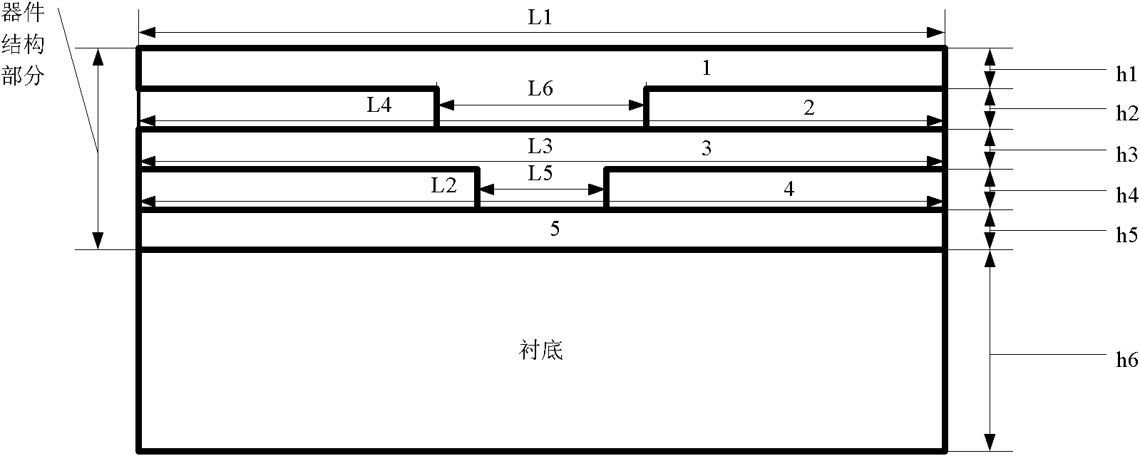
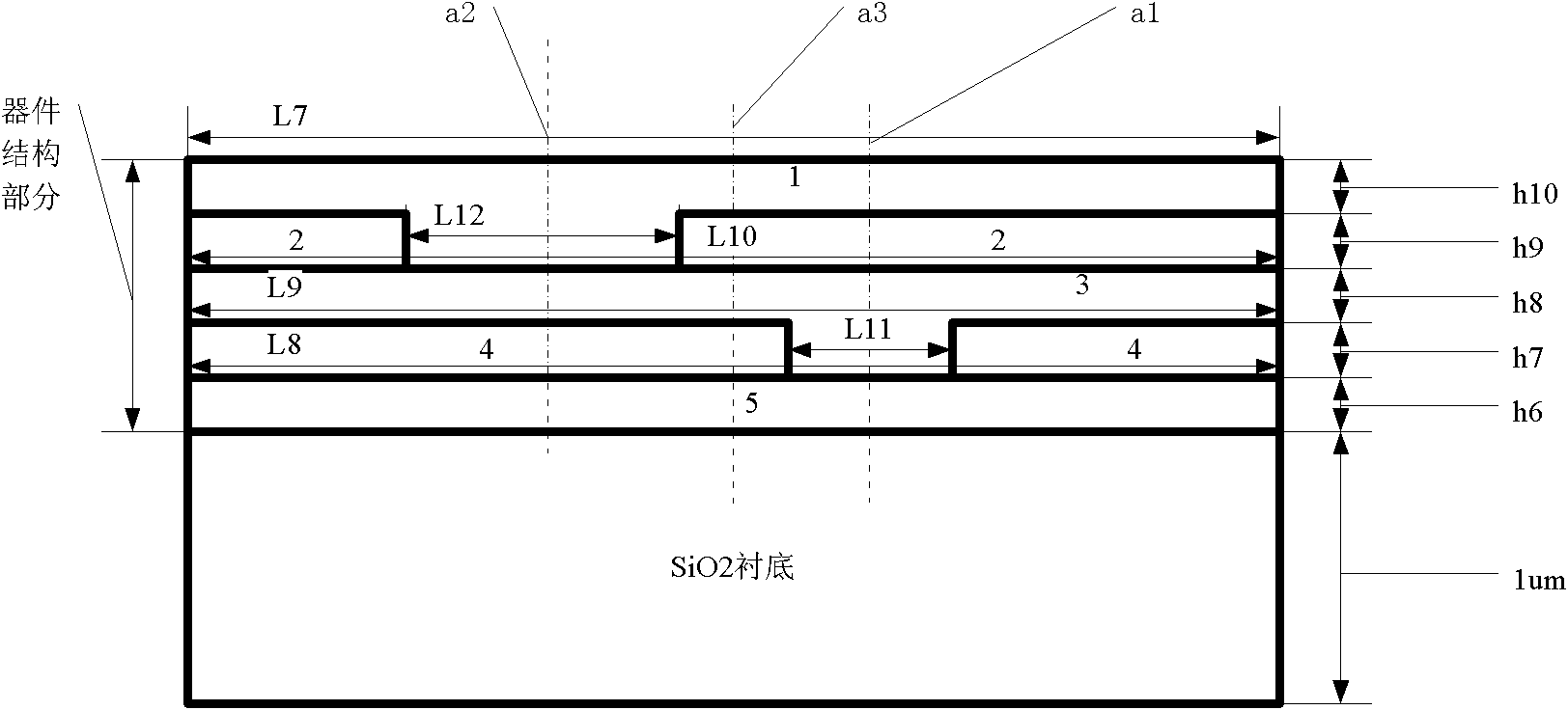
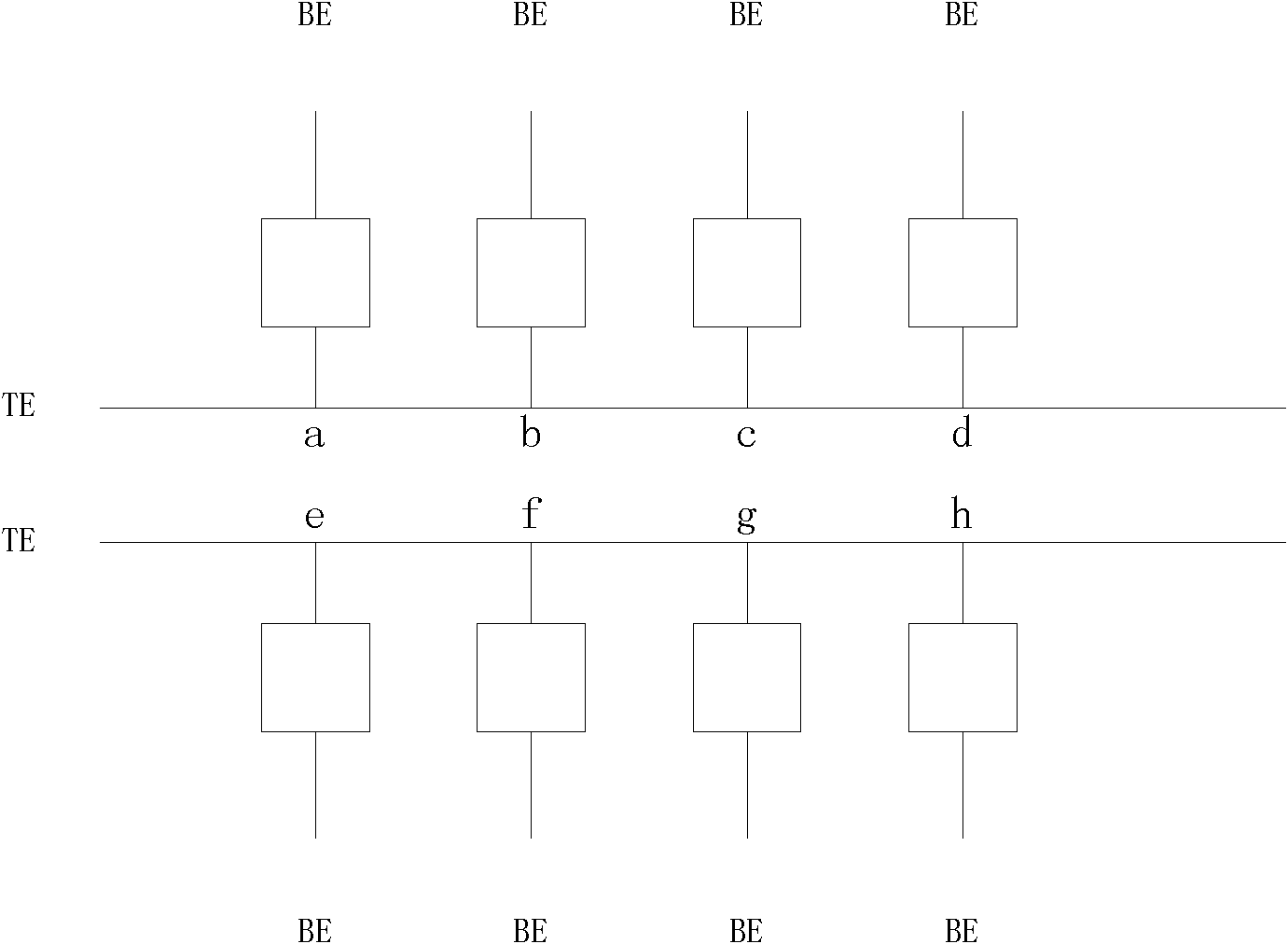
[0040] In this embodiment, the fabricated eight-cell asymmetric phase-change memory device is as image 3 Shown: a, b, c, d, e, f, g, h represent eight units respectively, TE represents the upper electrode, BE represents the lower electrode. Each unit can implement functions such as writing, reading and erasing. The cell structure of the asymmetric phase change memory device is as follows Figure 4 As shown: the lower electrode layer 5 is made of TiW, its width L7=12um, and its thickness h6=150nm.

[0041]The first insulating layer 4 is made of SiO2 material, its width L8=20um, and its thickness h7=200um. The first insulating layer 4 has a small hole with a width of L11 = 2um, and the central axis a1 of the small hole is horizontally shifted to the left by d1 = 1.5um relative to the central axis a3 on the lower electrode 5 .

[0042] The material used for the phase change layer 3 is Ge2Sb2Te5, its width L9=10um, and its thickness h8=150nm.

[0043] The second insulating la...

Embodiment 2

[0047] In this embodiment, an eight-unit asymmetric phase-change memory is manufactured, and the structure of the asymmetric phase-change memory unit is as follows Figure 5 As shown: the lower electrode layer 5 is made of Cu, its width L7=10um, and its thickness h6=100nm.

[0048] The first insulating layer 4 is made of TiO2 material, its width L8=15um, and its thickness h7=150um. The first insulating layer 4 has a small hole with a width of L11 = 1 um, and the central axis a1 of the small hole is horizontally shifted to the right by d1 = 1.5 um relative to the central axis a3 on the bottom electrode 5 .

[0049] The material used for the phase change layer 3 is Ge1Sb4Te7, its width L9=10um, and its thickness h8=100nm.

[0050] The second insulating layer 2 is made of TiO2 material, its width L10=20um, and its thickness h9=150nm. The second insulating layer 2 has a small hole with a width L12 = 2um, and the central axis a2 of the small hole is horizontally shifted to the le...

Embodiment 3

[0053] In this embodiment, the fabricated asymmetric phase-change memory device has a structure of an asymmetric phase-change memory cell such as Figure 6 As shown: the lower electrode layer 5 is made of Ag, its width L7=30um, and its thickness h6=500nm.

[0054] The first insulating layer 4 is made of amorphous Si material, its width L8=40um, and its thickness h7=500um. The first insulating layer 4 has a small hole with a width of L11 = 4um, and the central axis a1 of the small hole is horizontally shifted to the right by d1 = 4um relative to the central axis a3 on the lower electrode 5 .

[0055] The material used for the phase change layer 3 is GeTe. Its width L9=30um, thickness h8=500nm.

[0056] The second insulating layer 2 is made of amorphous Si material, its width L10=40um, and its thickness h9=500nm. The second insulating layer 2 has a small hole with a width of L12 = 6um, and the central axis a2 of the small hole is horizontally shifted to the left by d2 = 6um r...


PUM


Abstract

The invention belongs to an asymmetric phase-change memory unit and an element. The asymmetric phase-change memory unit comprises a lower electrode layer, a first insulation layer, a phase change layer, a second insulation layer and an upper electrode layer, which are overlapped from top down, wherein the first insulation layer has a small hole which is 10 nanometers to 4 micrometers wide; the phase change layer is contacted with the lower electrode layer through the small hole in the first insulation layer; the second insulation layer also has a small hole which is 10 nanometers to 5 micrometers wide; and an upper electrode is contacted with the phase change layer through the small hole in the second insulation layer. The core structural characteristic of the asymmetric phase-change memory unit lies in that any two of the axis of the small hole in the first insulation layer, the axis of the small hole in the second insulation layer and the axis of the lower electrode layer are not coincide. When the asymmetric phase-change memory unit and the element, which are provided by the invention, are used, a memory has a higher thermal property, and consequently, power consumption can be reduced while the original properties of the element are kept.

Description

technical field [0001] The invention belongs to phase-change memory technology, in particular to an asymmetric phase-change memory unit and device. Background technique [0002] Phase change memory technology was developed based on the rapid and reversible phase transition of chalcogenide compounds discovered by Ovshinsky in the late 1960s. Due to its significant advantages in data read and write speed, erasable times, device power consumption, component size and non-volatility, phase change memory is considered by the International Semiconductor Industry Association to be the most likely to replace the current flash memory and become the future memory Mainstream products and the first devices to become commercial products. [0003] The working principle of phase change memory is to use electric pulses to act on the device unit, so that the phase change material undergoes reversible phase transition between amorphous state and polycrystalline state, and realizes by distingu...

Claims


Application Information

Patent Timeline
Patent Type & Authority Patents(China)
IPC IPC(8): H01L45/00H01L27/24
Inventor 缪向水程晓敏鄢俊兵温学鑫孙巾杰瞿力文彭菊红
Owner HUAZHONG UNIV OF SCI & TECH
Why Eureka
Try Eureka