Metal oxide semiconductor (MOS) bootstrap switch circuit for calibrating sampling clock offset

A sampling clock and switching circuit technology, applied in the field of MOS bootstrap switching circuits, can solve the problems of increasing design complexity and chip area and power consumption

Active Publication Date: 2011-05-25
FUDAN UNIV
View PDF2 Cites 13 Cited by
  • Summary
  • Abstract
  • Description
  • Claims
  • Application Information

AI Technical Summary

Problems solved by technology

[0007] The main disadvantage of this technology is the need for an additional clock

Method used


Image

  • Metal oxide semiconductor (MOS) bootstrap switch circuit for calibrating sampling clock offset
  • Metal oxide semiconductor (MOS) bootstrap switch circuit for calibrating sampling clock offset
  • Metal oxide semiconductor (MOS) bootstrap switch circuit for calibrating sampling clock offset

Examples


specific Embodiment approach

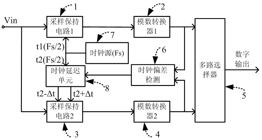
[0036] figure 2 Represents an implementation structure that can eliminate channel-to-channel sampling clock skew in a time-interleaved analog-to-digital converter. By detecting the clock deviation between channels, and then feeding it back to the clock delay circuit, the size and direction of the clock delay are adjusted until the deviation is finally eliminated. The invention saves the clock delay circuit unit and realizes the same function. The specific implementation is as follows:

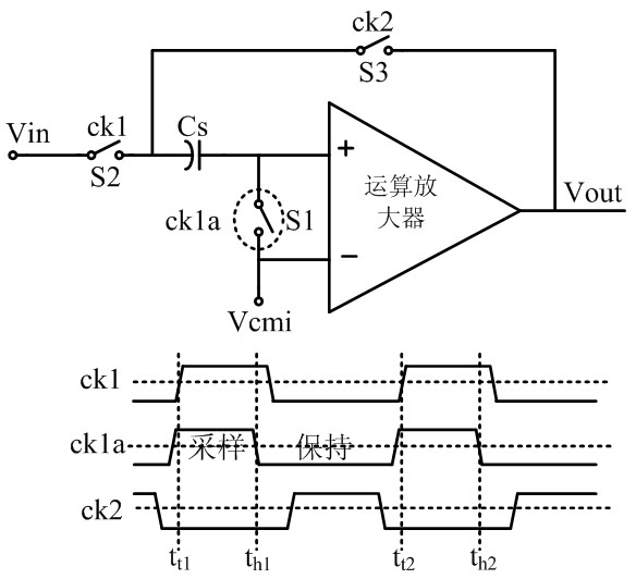
[0037] image 3 A schematic diagram of a single-ended sample-and-hold circuit. The timing diagrams of three clocks ck1, ck2 and ck1a are shown in the figure. at t t1 After time, the switches S1 and S2 are closed, S3 is opened, the circuit enters the sampling stage, and the capacitor Cs follows the input signal Vin. when the arrival time t h1 , the clock ck1a is turned off in advance, and this moment determines the actual sampling point of the sample-and-hold circuit. because t h1 In the...


PUM


Abstract

The invention belongs to the technical field of integrated circuits, and in particular relates to a metal oxide semiconductor (MOS) bootstrap switch circuit for calibrating sampling clock offset. The circuit is used for eliminating the sampling clock offset among channels of a time interleaving analog-digital converter. In the circuit, an MOSbootstrap switch is taken as a main body; a control signal is added to a bootstrap input end; and a control voltage signal is obtained by a clock offset detection module. A grid voltage bootstrapped circuit is used for bootstrapping a supply voltage for the control signal, so that the bootstrapped voltage follows with the control voltage signal. The bootstrapped voltage is added to the grid end of a switching tube so as to control the on and off of the switching tube. Thus, the control signal can adjust the on/off time of the switching tube, thereby effectively calibrating the clock offset and eliminating sampling mismatch among the channels.

Description

technical field [0001] The invention belongs to the technical field of integrated circuits, and in particular relates to a MOS bootstrap switch circuit for correcting sampling clock deviation. Background technique [0002] High-speed, high-precision and low-power analog-to-digital converters (ADCs) are widely used in wireless communication, instrument measurement, military radar and high-definition digital TV, etc., and are the development focus of today's mixed-signal system chip design. With the development of software-defined radio (SDR) communication technology, it is increasingly required that the digital part of the transceiver system be as close as possible to the antenna end, and the signal processing work after the intermediate frequency is all handed over to a digital processing chip that can be flexibly configured. Therefore, the analog-to-digital converter needs to sample in the intermediate frequency band or even the radio frequency band. The closer the A / D con...

Claims


Application Information

Patent Timeline
IPC IPC(8): H03K17/687
Inventor 任俊彦张鹏余北束晨王俊乾陈迟晓叶凡许俊李宁
Owner FUDAN UNIV
Why Eureka
Try Eureka