Fixture for solder paste printing and method for repairing integrated circuit board by utilizing same

An integrated circuit board and solder paste technology is applied in the field of printing solder paste fixtures and using the fixture to repair integrated circuit boards, which can solve the problems of difficulty in printing solder paste, partial damage to products, and high circuit board integration, and reduce repair costs. , The effect of solving the difficulty of printing solder paste and reducing the difficulty of repair

Inactive Publication Date: 2011-05-25
SHIN TECH ENG
View PDF4 Cites 4 Cited by
  • Summary
  • Abstract
  • Description
  • Claims
  • Application Information

AI Technical Summary

Problems solved by technology

Today's circuit boards are highly integrated, and the surrounding parts are too close to each other. It is very diffi

Method used


Image

  • Fixture for solder paste printing and method for repairing integrated circuit board by utilizing same
  • Fixture for solder paste printing and method for repairing integrated circuit board by utilizing same
  • Fixture for solder paste printing and method for repairing integrated circuit board by utilizing same

Examples


Embodiment Construction

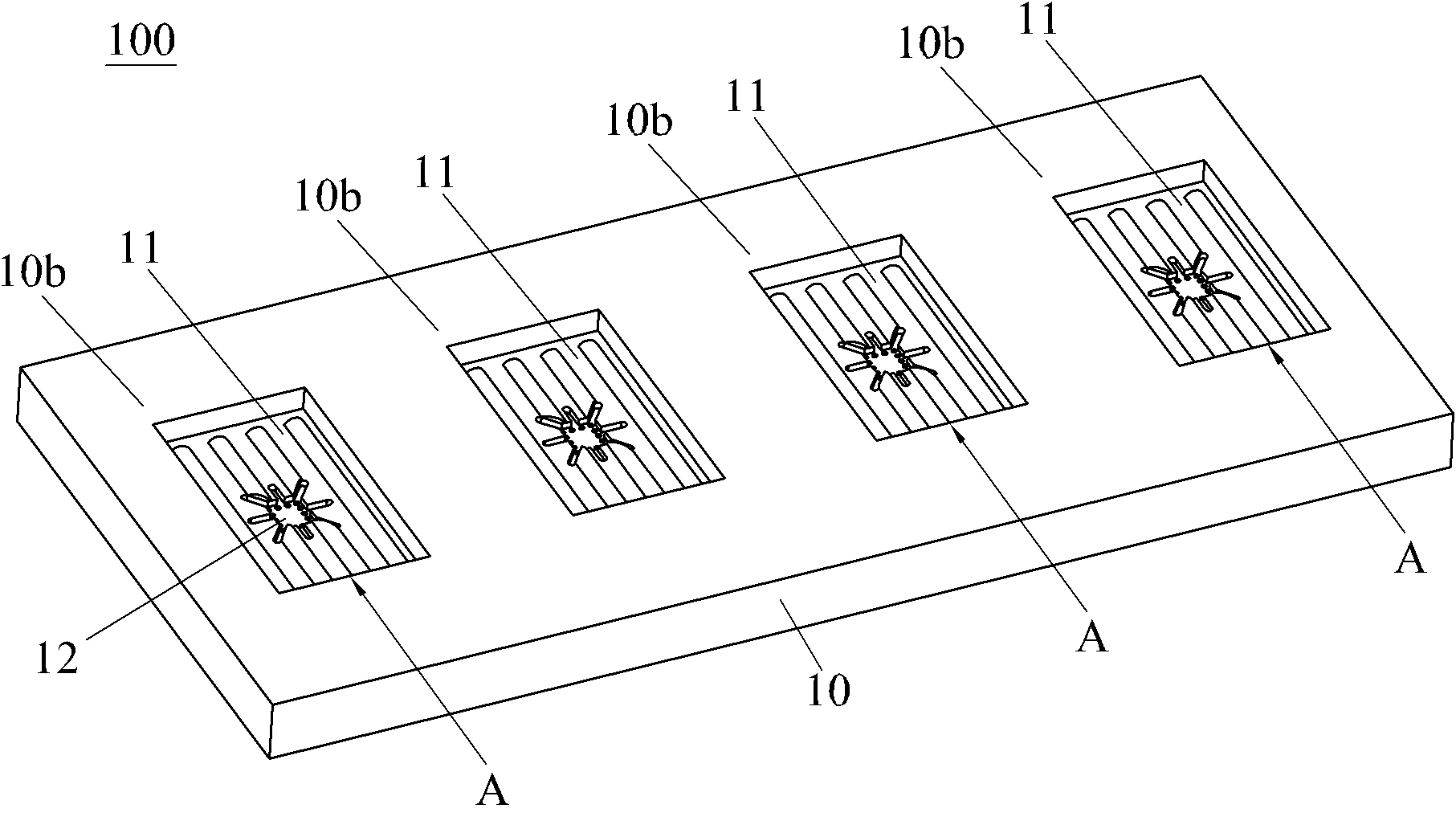
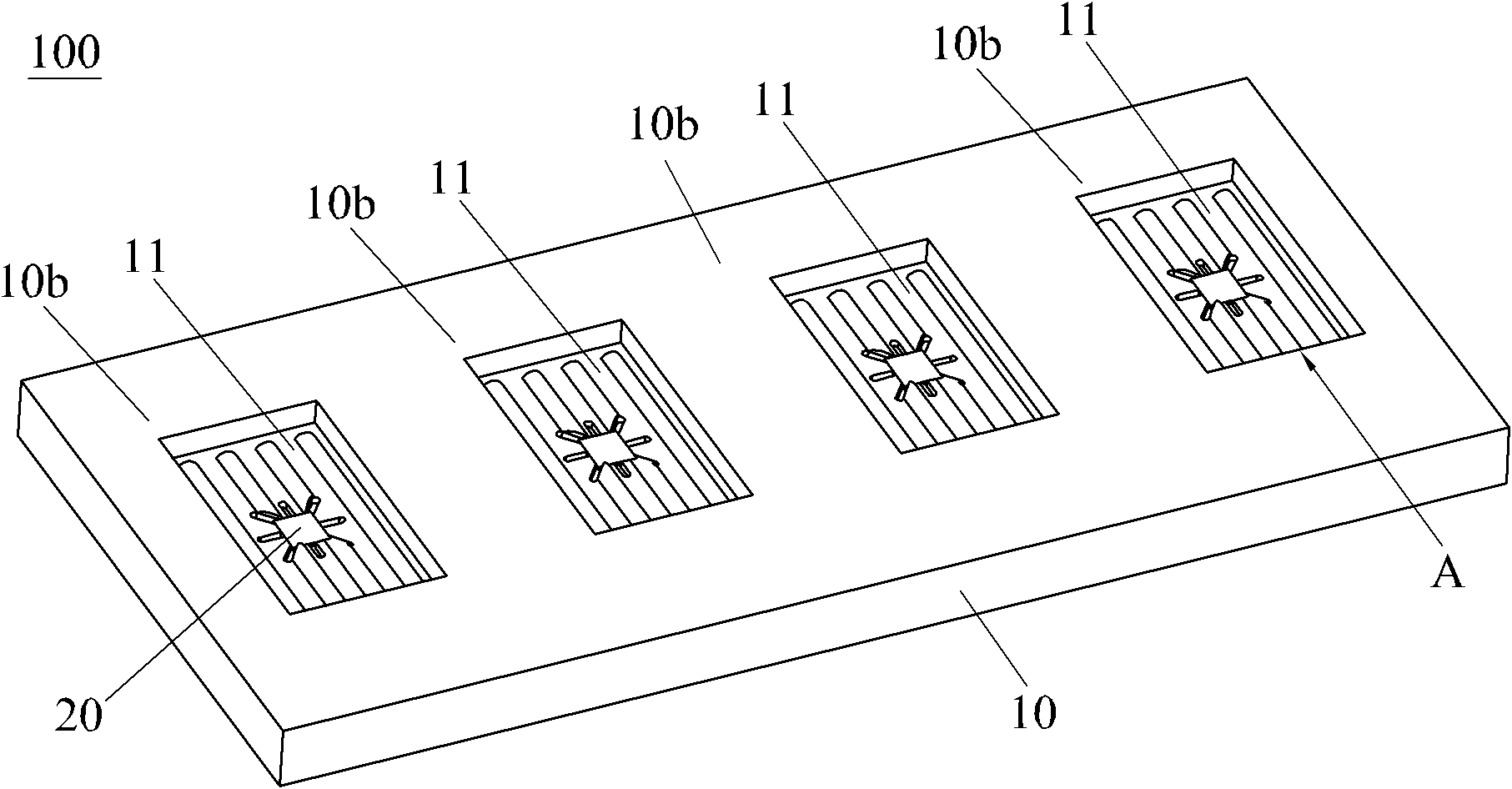
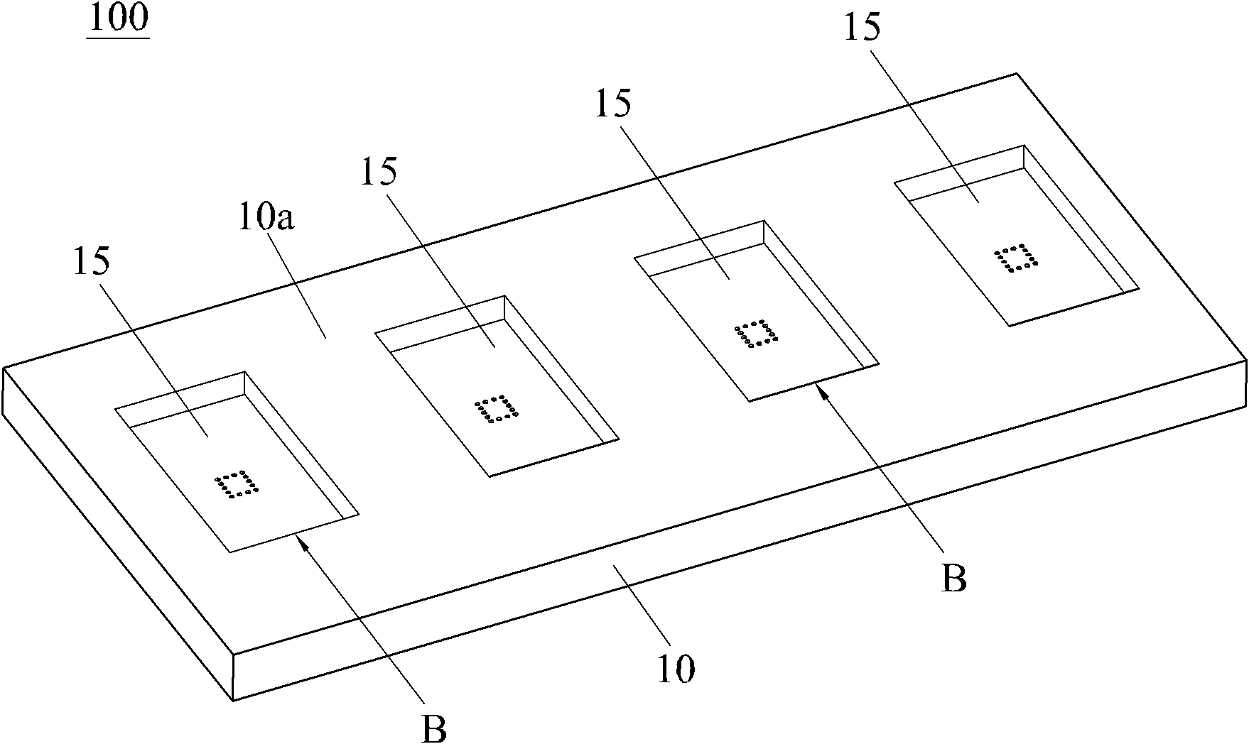
[0027] Embodiments of the present invention will now be described with reference to the drawings, in which like reference numerals represent like elements. As mentioned above, such as Figure 1-5 As shown, the printing solder paste jig 100 provided by the present invention includes a support plate 10, the front side 10b of the support plate 10 is provided with four chip accommodating grooves 11, and the back side 10a of the support plate 10 is recessed to form a soldering slot 15. The tin brushing slot 15 is directly opposite to the chip accommodating slot 11, and the bottom of the chip accommodating slot 11 is provided with a pin hole 13, and the pin hole 13 runs through the back of the support plate 10 10a, and the pin holes 13 correspond to the pins of the contained chip. Specifically, the pin hole 13 runs through the solder brush slot 15 and the chip accommodating slot 11 . The solder brush tank 15 is provided on the back side 10a of the support plate 10 to better hold t...


PUM


Abstract

The invention provides a fixture for solder paste printing, and the fixture is used for fixing a chip during solder paste printing. The fixture comprises a support plate, wherein, the front face of the support plate is equipped with a plurality of chip accommodating grooves, and the bottoms of the chip accommodating grooves are equipped with pin holes which are corresponding to the pins of the accommodated chips and penetrate through the rear face of the support plate. The fixture for solder paste printing has the advantages of lowering the repair difficulty and the repair cost, solving the difficulty in solder paste printing on a repair circuit board, and reducing the local damage degree of products caused by repair.

Description

technical field [0001] The invention relates to a fixture for fixing a chip when printing solder paste, in particular to a fixture for printing solder paste and a method for repairing an integrated circuit board using the fixture. Background technique [0002] In the 1990s, with the advancement of integration technology, the improvement of equipment and the use of deep submicron technology, large-scale integrated circuits, ultra-large-scale integrated circuits, and extremely large-scale integrated circuits appeared one after another, and the integration of silicon single chips continued to increase. The circuit packaging requirements are more stringent, the number of I / O pins has increased sharply, and the power consumption has also increased. In order to meet the needs of development, on the basis of the original packaging varieties, a ball grid array package is added, referred to as BGA (Ball Grid Array Package). In the 1990s, with the advancement of technology, the integ...

Claims


Application Information

Patent Timeline
IPC IPC(8): H05K3/34H01L21/50
Inventor 李小东明正东
Owner SHIN TECH ENG
Why Eureka
Try Eureka