Active array substrate, LCD panel and its mending method

A technology for liquid crystal display panels and array substrates, applied in optics, instruments, electrical components, etc., can solve problems such as poor contact of components and disconnection of data lines, and achieve the effect of improving production qualification rate and reducing repair difficulty.

Inactive Publication Date: 2009-05-13
AU OPTRONICS CORP
View PDF0 Cites 4 Cited by
  • Summary
  • Abstract
  • Description
  • Claims
  • Application Information

AI Technical Summary

Problems solved by technology

[0006] However, in the process, there may be phenomena such as poor contact of various components or defects such as disconnection of the data line 120. It can be seen from the known design that the above problems cannot be solved.

Method used


Image

  • Active array substrate, LCD panel and its mending method
  • Active array substrate, LCD panel and its mending method
  • Active array substrate, LCD panel and its mending method

Examples


Embodiment Construction

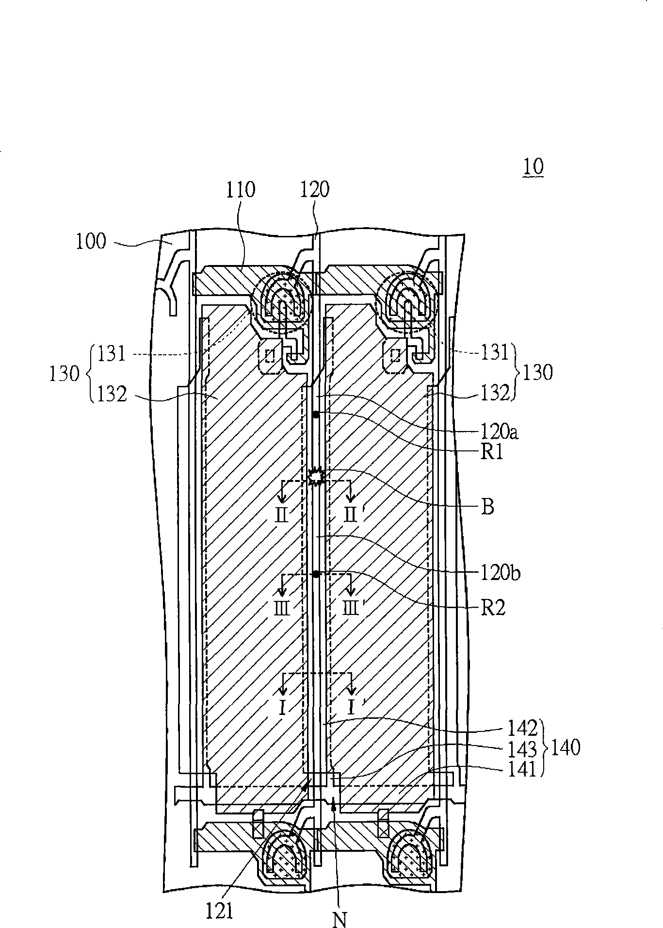
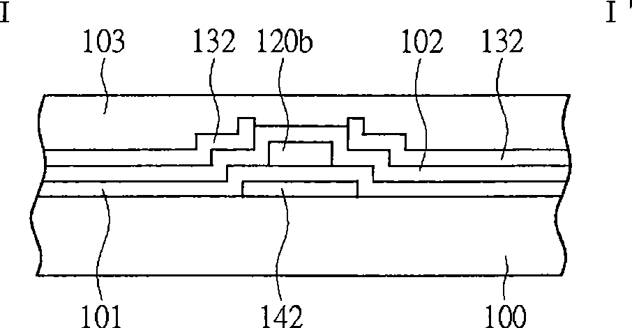
[0042] Figure 2A is a top view of an active matrix substrate according to an embodiment of the present invention, Figure 2B to Figure 2D respectively Figure 2A From the schematic cross-sections of I-I', II-II' and III-III', Figure 2E for Figure 2A Partial enlarged view of region N viewed from the lateral direction of the substrate.

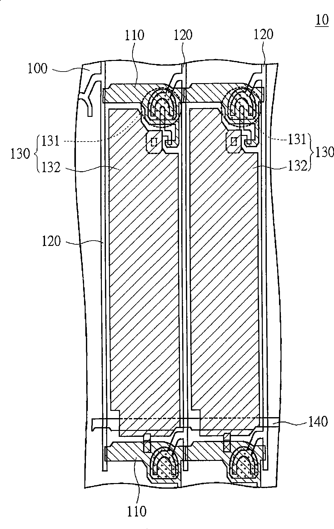
[0043] Please refer to Figure 2A The active array substrate 10 includes a substrate 100 , scan lines 110 , data lines 120 , pixel units 130 and common electrodes 140 . For convenience, only two pixel units are shown as an example, but it is not intended to limit the present invention. The scan lines 110 are disposed on the substrate 100 , and the data lines 120 are disposed on the substrate 100 and are substantially parallel to the plurality of scan lines 110 . The pixel units 130 are respectively connected to the plurality of scanning lines 110 and the plurality of data lines 120 correspondingly, each pixel unit 130 has a switching el...


PUM


Abstract

The invention provides an active array basal plate, a liquid crystal display panel and a mending method thereof. The active array basal plate comprises a substrate, a plurality of scanning beams, a plurality of digital beams, a plurality of pixel units and a common electrode, wherein the common electrode is provided with a main body part, a branch part and a neck part, the branch part is overlapped with at least one of the digital beams and a pixel electrode of the two adjacent pixel units corresponding to the digital beam. The mending method of the invention is more convenient and rapid, and furthermore, the production yield is increased, and the mending difficulty is reduced.

Description

technical field [0001] The invention relates to an active array substrate, a liquid crystal display panel and a repairing method thereof, in particular to an active array substrate capable of repairing defective data lines, a liquid crystal display panel and a repairing method thereof. Background technique [0002] Flat panel displays are currently being developed as the most commonly used display products, such as liquid crystal displays. Liquid crystal displays have the advantages of thinness and low radiation, and are therefore widely used in the market. [0003] The TFT liquid crystal display is composed of an active matrix substrate, an opposite substrate and a liquid crystal layer. The active array substrate generally consists of a plurality of thin film transistors arranged in an array, a plurality of data lines, a plurality of scanning lines, and pixel electrodes correspondingly configured and connected to each thin film transistor. The thin film transistor is used ...

Claims


Application Information

Patent Timeline
Patent Type & Authority Applications(China)
IPC IPC(8): H01L27/12H01L23/522H01L21/768G02F1/1362G02F1/1343G02F1/13
Inventor 林宗正樊祥彬
Owner AU OPTRONICS CORP
Why Eureka
Try Eureka