Active array substrate, LCD panel and its mending method
A technology for liquid crystal display panels and array substrates, applied in static indicators and other directions, can solve problems such as disconnection of data lines and poor contact of components, and achieve the effect of improving production qualification rate and reducing repair difficulty.
- Summary
- Abstract
- Description
- Claims
- Application Information
AI Technical Summary
Problems solved by technology
Method used
Image
Examples
Embodiment Construction
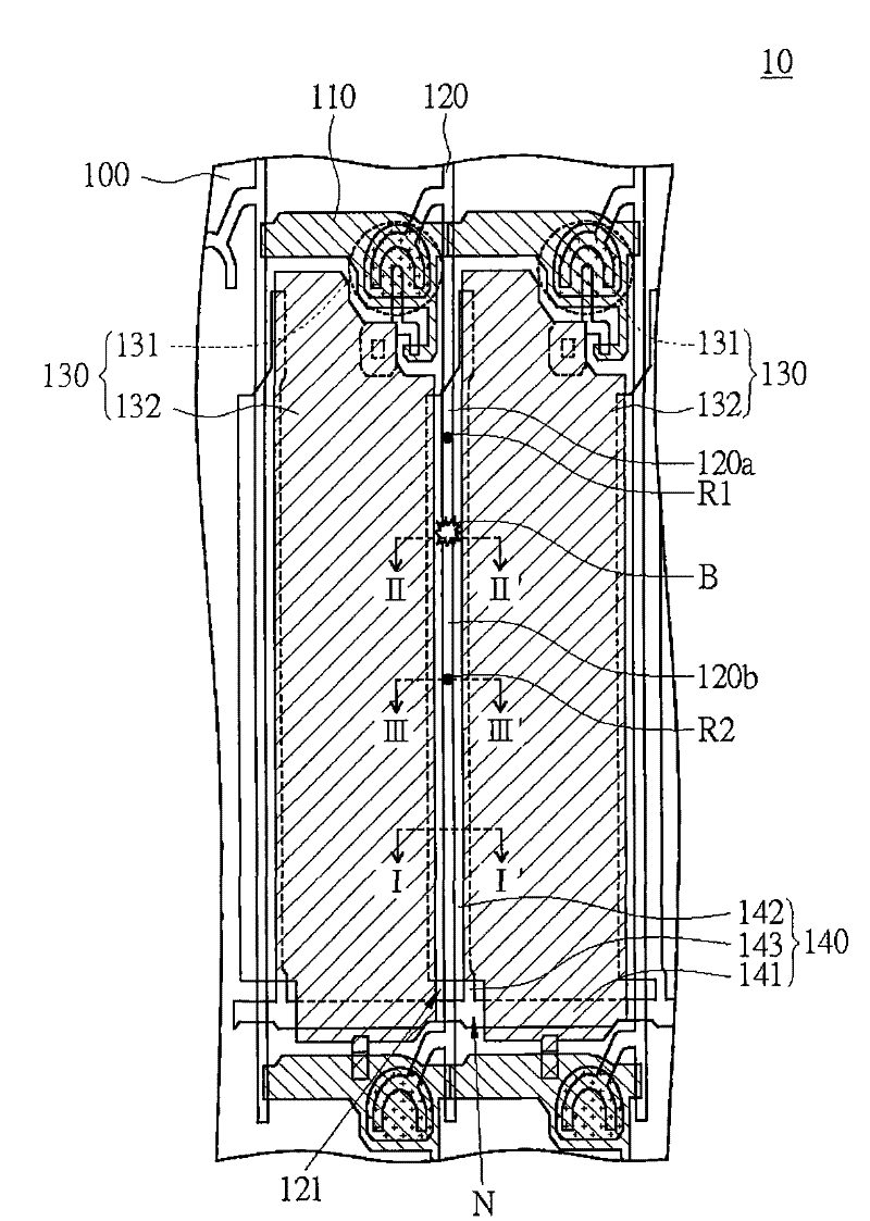
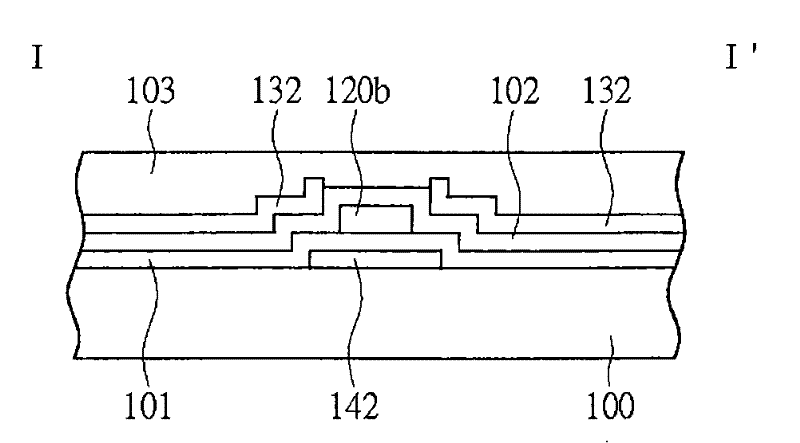
[0042] Figure 2A is a top view of an active matrix substrate according to an embodiment of the present invention, Figure 2B to Figure 2D respectively Figure 2A From the schematic cross-sections of I-I', II-II' and III-III', Figure 2E for Figure 2A Partial enlarged view of region N viewed from the lateral direction of the substrate.
[0043] Please refer to Figure 2A The active array substrate 10 includes a substrate 100 , scan lines 110 , data lines 120 , pixel units 130 and common electrodes 140 . For convenience, only two pixel units are shown as an example, but it is not intended to limit the present invention. The scan lines 110 are disposed on the substrate 100 , and the data lines 120 are disposed on the substrate 100 and are generally perpendicular to the plurality of scan lines 110 . The pixel units 130 are respectively connected to the plurality of scanning lines 110 and the plurality of data lines 120 correspondingly, each pixel unit 130 has a switching e...
PUM
 Abstract
Description
Claims
Application Information


