Wafer processing device

A technology for processing devices and wafers, which is applied in the direction of electrolytic components, cells, and electrolytic processes. It can solve the problems of large space required for wafer processing devices, inability to meet large-scale production, and endangering workers' health, so as to eliminate harm to workers. Physical health, improving work efficiency and production pass rate, improving production efficiency and production pass rate

Active Publication Date: 2013-04-17
SHANGHAI SINYANG SEMICON MATERIALS
View PDF9 Cites 11 Cited by
  • Summary
  • Abstract
  • Description
  • Claims
  • Application Information

AI Technical Summary

Problems solved by technology

[0003] However, in the prior art, a series of procedures of the wafer processing device need to be manually operated. On the one hand, it will reduce production efficiency and increase production costs. On the other hand, improper manual operation will cause damage to the wafer and reduce the production pass rate.
At the same time, due to the manual operation, the wafer processing device requires a large space and the space utilization rate is low
Another disadvantage of manual operation is that it is labor-intensive and inefficient, which cannot meet the needs of mass production
Manual operation will also cause workers to come into contact with the electroplating solution and endanger the health of workers

Method used


Image

  • Wafer processing device
  • Wafer processing device
  • Wafer processing device

Examples


Embodiment Construction

[0052] The present invention is described in detail below in conjunction with accompanying drawing:

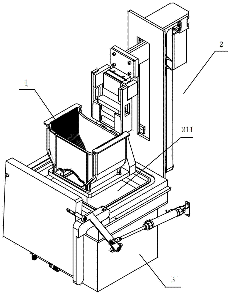
[0053] Such as figure 1 As shown, the wafer processing device includes a grab lifting device 2 and a processing tank 3; the processing tank 3 is provided with a sealable cavity 311, which is used to hold a processing liquid to process the wafer; grab The lifting device 2 is arranged on one side of the processing tank 3 and is used for transporting the wafer into the chamber 311 .

[0054] Such as figure 1 As shown, the wafer processing device also includes a wafer storage tank 1 for storing wafers to realize batch processing of wafers.

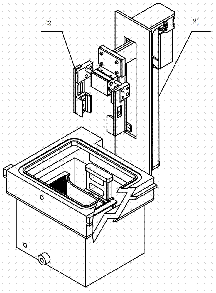
[0055] Such as figure 2As shown, it is the grasping and lifting device 2 of the wafer processing device, including the lifting device 21 and the grasping device 22; Lifting movement.

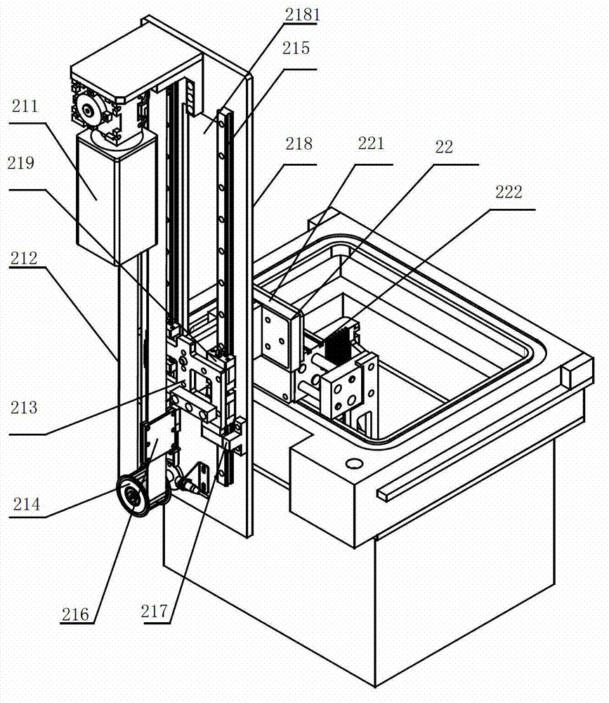
[0056] Such as image 3 As shown, the lifting device 21 of the wafer processing device includes a fixed base plate 218, a transmission device 212 and a l...


PUM


Abstract

The invention discloses a wafer processing device, which is characterized by comprising a processing tank and provided with an accommodating cavity which can be sealed, wherein the accommodating cavity is used for accommodating treatment fluid to process wafers; and a grabbing and lifting device, arranged on one side of the processing tank for conveying the wafers to the accommodating cavity of the processing tank. According to the wafer processing device provided by the invention, the automatic operation of a series of working procedures is achieved by the combination of the grabbing and lifting device and the processing tank, the work efficiency is greatly enhanced, the labor cost is saved, and the qualified rate is improved.

Description

technical field [0001] The invention relates to a wafer processing device, in particular to an automatic wafer processing device. Background technique [0002] During the wafer production process, processes such as wetting, electroplating, and etching are required. Blind vias are formed on the wafer surface. Gas is easy to store in the blind holes on the wafer surface. If a wafer with blind vias is placed directly into the electroplating solution, the residual gas in the blind holes will prevent the electroplating solution from entering the blind vias. Due to the small size of the blind hole and the high surface tension of the electroplating solution, it is also difficult for the electroplating solution to enter the blind hole. If the blind holes of the wafer cannot be electroplated, the quality of wafer electroplating will be seriously affected. Therefore, in order to improve the quality of electroplating, it is necessary to vacuumize the wafer to remove the gas in the ...

Claims


Application Information

Patent Timeline
Patent Type & Authority Applications(China)
IPC IPC(8): C25D7/12C25D17/00C25D21/00
Inventor 王振荣刘红兵陈概礼
Owner SHANGHAI SINYANG SEMICON MATERIALS
Why Eureka
Try Eureka