Optical proximity effect corrective modeling method and generating method of test pattern

A technology of optical proximity effect and test pattern, which is applied in the field of photolithography, can solve the problems of poor photolithography quality of optical proximity effect test pattern, etc.

Active Publication Date: 2011-06-08
CSMC TECH FAB2 CO LTD
View PDF1 Cites 9 Cited by
  • Summary
  • Abstract
  • Description
  • Claims
  • Application Information

AI Technical Summary

Problems solved by technology

[0006] In order to solve the problem of poor photolithography quality of the optical proximity effect test pattern after lithography on the wafer in the traditional process for critical dimensions below 130nm, it is necessary

Method used


Image

  • Optical proximity effect corrective modeling method and generating method of test pattern
  • Optical proximity effect corrective modeling method and generating method of test pattern
  • Optical proximity effect corrective modeling method and generating method of test pattern

Examples


Embodiment Construction

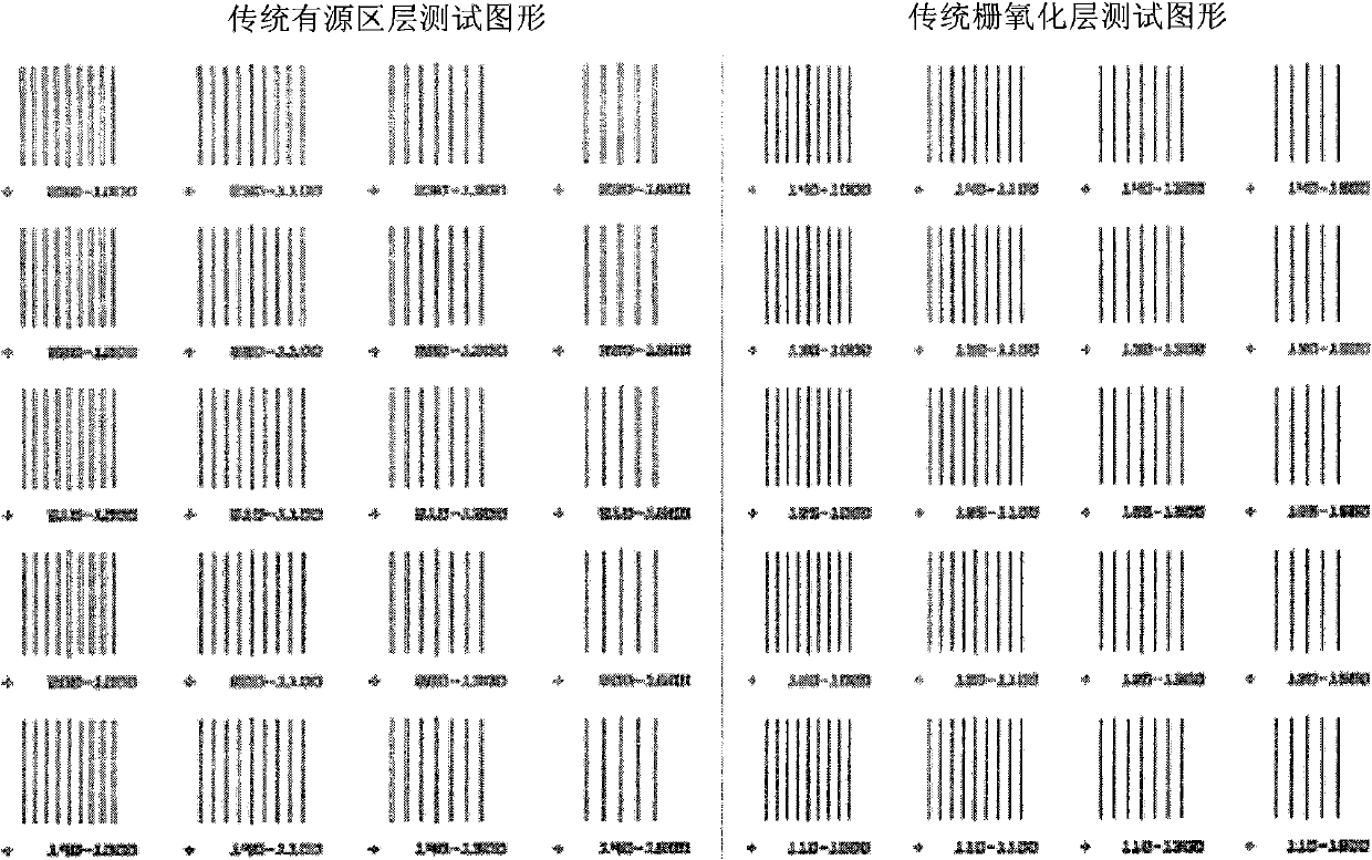
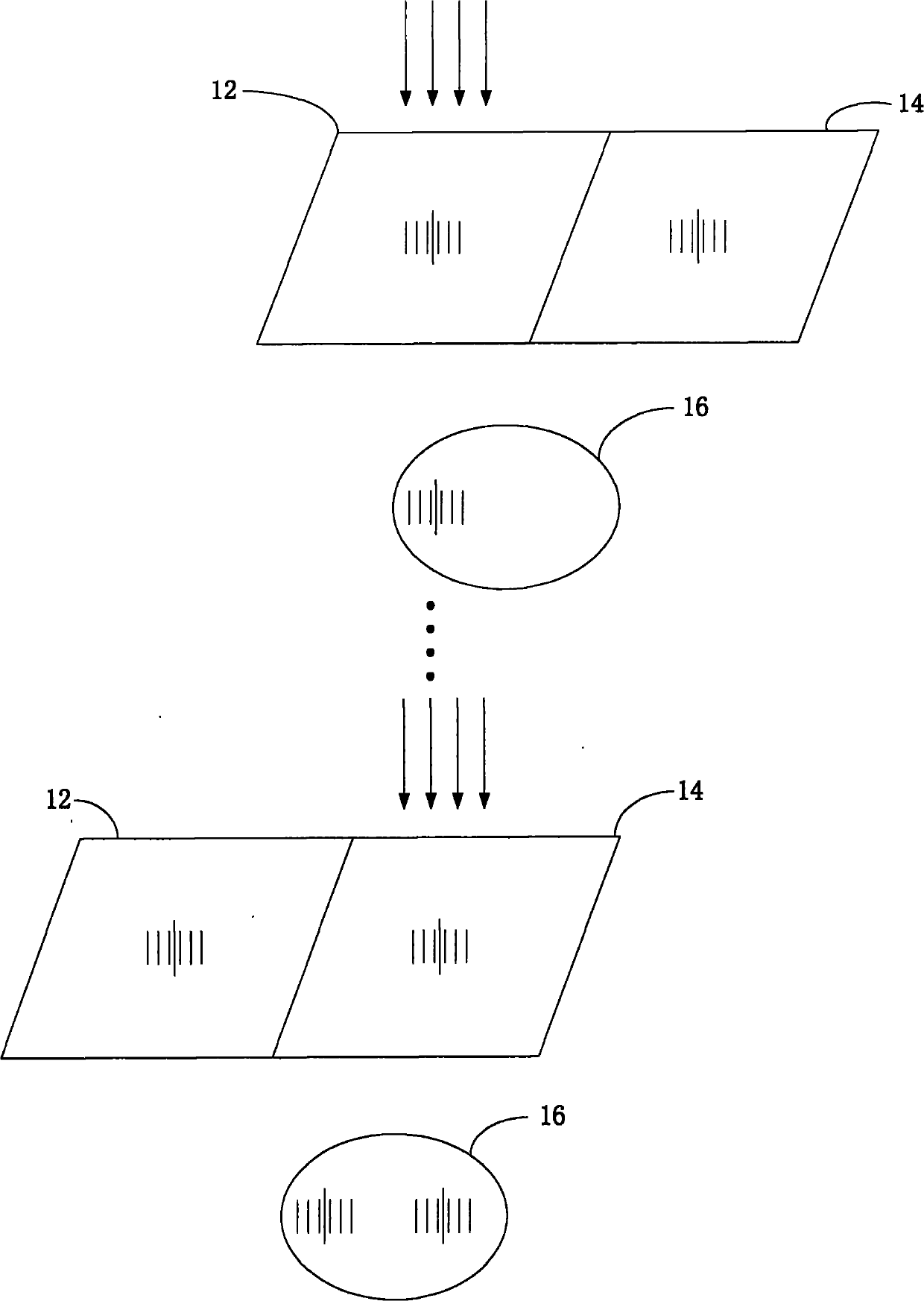
[0024] The method for forming the optical proximity effect test pattern in the preferred embodiment of the present invention is to regenerate a group of enlarged patterns on the basis of the original test patterns of each traditional level. The enlarged pattern is obtained by enlarging one or several groups of test patterns in the original test patterns, such as Figure 4 shown. In this way, after photoetching the optical proximity effect test pattern of the preferred embodiment of the present invention onto the mask plate, each layer of the test pattern has two areas, the original pattern area and the enlarged pattern area.

[0025] The present invention will be clearly and completely described below by taking the active region layer and the gate oxide layer as examples. The purpose of generating enlarged graphics is to simulate the real circuit layout situation. After photoetching the optical proximity effect test pattern of the active region layer onto the wafer, the orig...


PUM


Abstract

The invention relates to a generating method of a test pattern of optical proximity effect, and the method includes steps of: amplifying each layer of the original test pattern to obtain an amplified pattern; photoetching the original test pattern and the amplified pattern on a mask plate to form an original pattern region and an amplified pattern region respectively; and photoetching the original pattern region and the amplified pattern region which are on the mask plate on a wafer. The invention also relates to a model based optical proximity effect corrective modeling method of a test pattern generated by the above method. The invention truly simulates the condition that gate oxide covers on a layer of active region, and truly reflects optical proximity effect of overlapping lithography between gate oxide and the layer of active region. Patterns with very good quality are obtained on the wafer, and thus high quality optical proximity effect correction can be carried out.

Description

【Technical field】 [0001] The invention relates to photolithography technology in the semiconductor industry, in particular to a method for forming an optical proximity effect test pattern, and also to a model-based modeling method for optical proximity effect correction. 【Background technique】 [0002] Optical proximity effect (Optical Proximity Effect, OPE) refers to that when the light beam passes through the pattern on the mask and projects on the wafer, on the one hand, diffraction occurs, and on the other hand, it is reflected back by the semiconductor substrate of the wafer to cause interference. Therefore, optical proximity correction (Optical ProximityCorrection, OPC) needs to be performed on the mask pattern. [0003] Optical proximity correction is generally divided into rule-based (Rule based OPC) and model-based (Model based OPC). The latter has a modeling process, the basic process of which is to photoetch a set of pre-designed test patterns on the wafer, and c...

Claims


Application Information

Patent Timeline
IPC IPC(8): G03F1/14G06F17/50G03F1/36
Inventor 黄旭鑫王谨恒张雷
Owner CSMC TECH FAB2 CO LTD
Why Eureka
Try Eureka