Method for manufacturing layers required by integrated circuit layout registration

A technology of integrated circuits and manufacturing methods, which is applied in the fields of electrical digital data processing, special data processing applications, instruments, etc., and can solve problems such as the inability to guarantee the accuracy of graphic splicing, the inability to process image splicing, and the inability to complete graphics, etc.

Inactive Publication Date: 2015-02-25
SUZHOU R&D CENT OF NO 214 RES INST OF CHINA NORTH IND GRP
View PDF3 Cites 1 Cited by
  • Summary
  • Abstract
  • Description
  • Claims
  • Application Information

AI Technical Summary

Problems solved by technology

[0003] The registration of integrated circuit layout belongs to a kind of industrial property rights in intellectual property rights. During the registration, it is necessary to make graphics at each level. The graphics are generally obtained by taking screenshots of integrated circuit layouts and then manually splicing them. This method It is suitable for small-area layouts, but for layouts designed with deep submicron technology or large-area layouts, since there are requirements for the registered layout enlargement ratio, and the gr

Method used


Image

  • Method for manufacturing layers required by integrated circuit layout registration
  • Method for manufacturing layers required by integrated circuit layout registration

Examples


Embodiment Construction

[0018] The present invention will be further described below in conjunction with the accompanying drawings. The following examples are only used to illustrate the technical solution of the present invention more clearly, but not to limit the protection scope of the present invention.

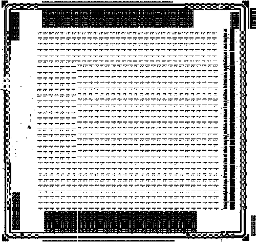
[0019] Taking the layout of a certain chip as an example, the chip adopts 0.35μm2P3M process, 15 layers, and the chip area is 6.83mm×6.43mm.

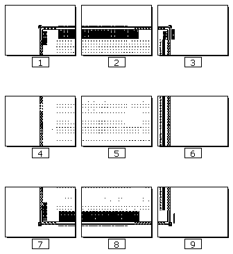
[0020] 1. Layout level flattening: According to the gds format data file of the chip layout, import the file, open the general diagram of the chip layout, and select the flattening command to flatten the units of its hierarchical design. The flattened general diagram contains 15 layers of graphics from L1 to L15;

[0021] 2. Printing settings: Select a certain layer with technological characteristics such as contact hole layer L8, set appropriate printing parameters according to the size of the chip layout, such as printing ratio, number of printed sheet...


PUM


Abstract

The invention discloses a method for manufacturing layers required by integrated circuit layout registration. The method includes the following steps that a data file of the gds format of an integrated circuit layout is introduced into planishing; a certain layer with process features is selected, and the layer is printed to form an electronic document file; the page margins of pages of picture files are set sequentially, graphs unrelated to the layout graphs are removed, only the layout graphs are reserved, and the adjacent layout graphs to be spliced are made to be right aligned with the page margins and are converted into a plurality of files of the jpeg format of the layer; the files of the jpeg format of the layer are selected, shapes of chip layouts are compared, the corresponding positions of the files of the jpeg format are set and are spliced into a graphic file; the spliced graphic file is evaluated; the manufactured files of all the layers are gathered to one file, and the layer files for the integrated circuit layout registration are formed. By means of the method, the splicing workload is lowered, the splicing accuracy is improved, and the requirement for layer manufacturing is met.

Description

[0001] technical field [0002] The invention relates to a method for making layers required for integrated circuit layout registration, and belongs to the technical field of integrated circuits. Background technique [0003] The registration of integrated circuit layout belongs to a kind of industrial property rights in intellectual property rights. During the registration, it is necessary to make graphics at each level. The graphics are generally obtained by taking screenshots of integrated circuit layouts and then manually splicing them. This method It is suitable for small-area layouts, but for layouts designed with deep submicron technology or large-area layouts, since there are requirements for the registered layout enlargement ratio, and the graphics must be clearly visible and undistorted when taking screenshots, manual The screenshot method needs to capture a lot of pictures, which leads to a lot of work when using manual stitching and the accuracy of graphic stitch...

Claims


Application Information

Patent Timeline
IPC IPC(8): G06F17/50
Inventor 吕江萍杨林敏刘彬刘霞王丽丽陈超
Owner SUZHOU R&D CENT OF NO 214 RES INST OF CHINA NORTH IND GRP
Why Eureka
Try Eureka