Direct-writing photoetching machine splicing method

A direct-writing, lithography machine technology, applied in semiconductor lithography machine graphics image processing, graphics splicing, and computer graphics development, can solve problems such as unsatisfactory customers, slow production capacity, etc., to improve splicing accuracy and reduce self-precision needs, the effect of improving graphics quality

Inactive Publication Date: 2019-12-03
HEFEI CHIP FOUND MICROELECTRONICS EQUIP CO LTD
View PDF3 Cites 1 Cited by
  • Summary
  • Abstract
  • Description
  • Claims
  • Application Information

AI Technical Summary

Problems solved by technology

However, when the height of the graphics is getting higher and higher, the scanning time will be longer under the same scanning times and speed, and the production capacity will be very slow, which cannot meet the needs of customers.

Method used


Image

  • Direct-writing photoetching machine splicing method
  • Direct-writing photoetching machine splicing method
  • Direct-writing photoetching machine splicing method

Examples


Embodiment Construction

[0030] In order to further illustrate the features of the present invention, please refer to the following detailed description and accompanying drawings of the present invention. The accompanying drawings are for reference and description only, and are not intended to limit the protection scope of the present invention.

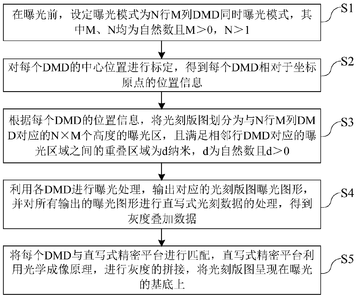
[0031] Such as Figure 1 to Figure 4 As shown, this embodiment discloses a splicing method for a direct-writing lithography machine, including the following steps S1-S5:

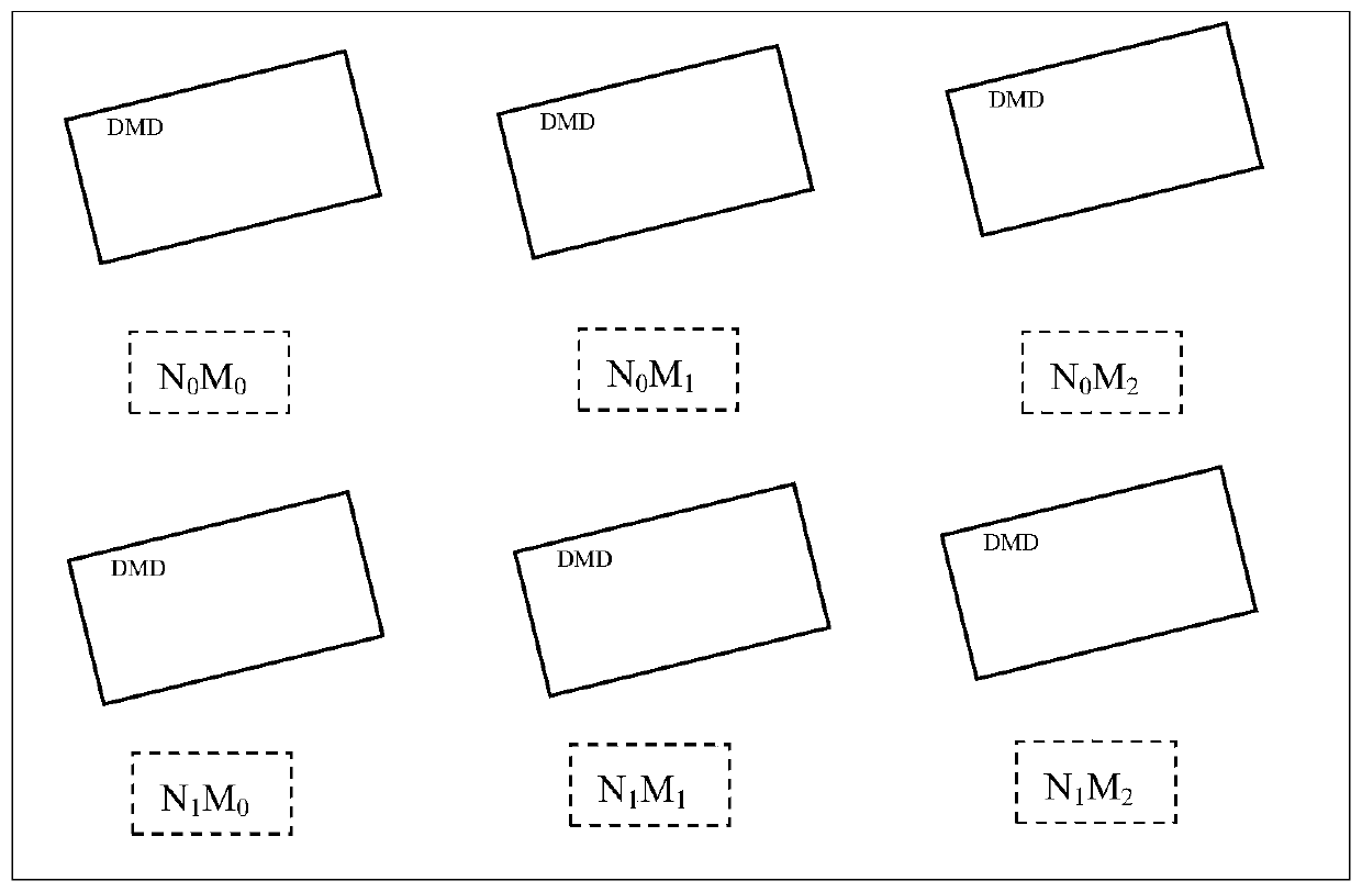
[0032] S1. Before exposure, set the exposure mode to N rows and M columns DMD simultaneous exposure mode, where M and N are natural numbers and M>0, N>1;

[0033] S2. Calibrate the center position of each DMD to obtain the position information of each DMD relative to the coordinate origin;

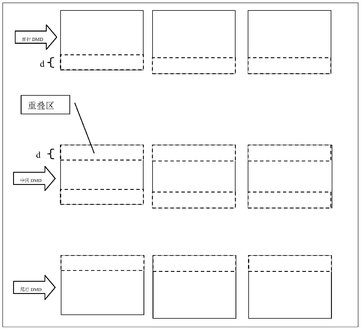
[0034] S3. According to the position information of each DMD, divide the lithography layout into exposure areas of N×M heights corresponding to N rows and M columns of DMDs, and satisfy the requireme...


PUM


Abstract

The invention discloses a direct-writing photoetching machine splicing method, and belongs to the semiconductor photoetching machine graph and image processing and splicing technology field. The method comprises the following steps of before exposure, setting an exposure mode as an N-row M-column DMD simultaneous exposure mode; dividing a photoetching layout into N * M height exposure areas corresponding to the N-row M-column DMD, wherein an overlapping area between the exposure areas corresponding to adjacent rows of DMDs is d nanometers; carrying out exposure processing by using each DMD, and carrying out direct-writing photoetching data processing on all output exposure graphs to obtain gray level superposition data; matching each DMD with a direct-writing precision platform, wherein the direct-writing precision platform uses an optical imaging principle to carry out gray scale splicing, and the photoetching layout is presented on an exposed substrate. In the method, N-row M-columnDMD simultaneous exposure is adopted, splicing precision is improved through splicing of gray-scale maps, possibility of segmented exposure of photoetching patterns is achieved, and productivity is improved.

Description

technical field [0001] The invention relates to the technical fields of graphic image processing, graphic splicing, and computer graphics development of a semiconductor lithography machine, in particular to a splicing method for a direct-write lithography machine. Background technique [0002] Direct-write lithography technology is a technology that prints characteristic patterns on the surface of photosensitive materials (mostly glue or film). Among them, maskless lithography technology uses digital micromirror system to generate patterns. The resulting magnification is projected onto a light-sensitive substrate, producing a pattern of features. [0003] Maskless lithography can effectively reduce the complexity of the lithography system (no mask stage, mask transfer, simple frame structure) and mask processing and maintenance costs. It is one of the development trends for large-scale substrate lithography . The maskless lithography method based on the Spatial Light Modul...

Claims


Application Information

Patent Timeline
Patent Type & Authority Applications(China)
IPC IPC(8): G03F7/20
CPCG03F7/70291G03F7/70475
Inventor 赵美云
Owner HEFEI CHIP FOUND MICROELECTRONICS EQUIP CO LTD
Why Eureka
Try Eureka