Semiconductor structure forming method and semiconductor structure

A technology of semiconductors and inorganic components, applied in semiconductor/solid-state device manufacturing, electrical components, circuits, etc., can solve problems such as semiconductor structure performance needs to be improved, achieve the effect of improving graphic quality, avoiding tilt or collapse, and improving production yield

Pending Publication Date: 2020-10-16
CHANGXIN MEMORY TECH INC
View PDF0 Cites 1 Cited by
  • Summary
  • Abstract
  • Description
  • Claims
  • Application Information

AI Technical Summary

Problems solved by technology

[0004] However, the performance of semiconductor structures

Method used


Image

  • Semiconductor structure forming method and semiconductor structure
  • Semiconductor structure forming method and semiconductor structure
  • Semiconductor structure forming method and semiconductor structure

Examples


Embodiment Construction

[0015] It can be seen from the background art that the performance of the existing semiconductor structures needs to be improved.

[0016] Now combined with a method of forming a semiconductor structure for analysis, Figure 1 to Figure 4 It is a schematic diagram of a cross-sectional structure corresponding to each step of a method for forming a semiconductor structure.

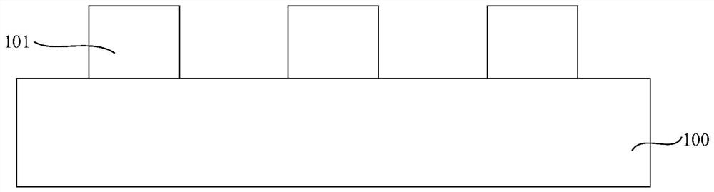
[0017] refer to figure 1 , providing a substrate 100 on which several discrete sacrificial layers 101 are formed.

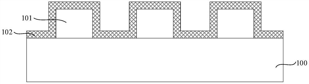
[0018] refer to figure 2 , forming a side wall film 102 on the top and side walls of the sacrificial layer 101 and the base, and the side wall film 102 conformally covers the sacrificial layer 101 .

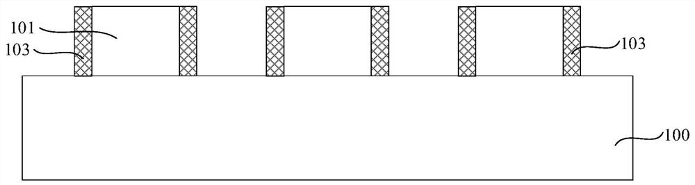
[0019] refer to image 3 , etch back (etch back) the sidewall film 102 (refer to figure 2 ), etch and remove the sidewall film 102 on the top of the sacrificial layer 101 , and also etch and remove the sidewall film 102 on the substrate 100 to form a sidewall layer 103 covering the sidewall...


PUM

PropertyMeasurementUnit
Thicknessaaaaaaaaaa

Abstract

The embodiment of the invention relates to a forming method of a semiconductor structure, and the semiconductor structure. The forming method comprises the steps: providing a substrate, and forming aplurality of discrete sacrificial layers on the substrate; forming a buffer layer on the surface of the side wall of the sacrificial layer, wherein the material of the buffer layer contains organic groups and inorganic components; forming a side wall layer on the surface of the buffer layer, wherein the buffer layer is located between the side wall layer and the sacrificial layer; after the side wall layer is formed, removing the sacrificial layer; and after the sacrificial layer is removed, etching the substrate by taking the side wall layer and the buffer layer as masks. According to the invention, the pattern quality of the self-aligned pattern can be improved, and the semiconductor production yield is improved.

Description

technical field [0001] Embodiments of the present invention relate to the field of semiconductor technology, and in particular, to a method for forming a semiconductor structure and the semiconductor structure. Background technique [0002] Semiconductor technology continues to move towards smaller process nodes driven by Moore's Law. With the continuous advancement of semiconductor technology, the functions of devices are becoming more and more powerful, and the difficulty of semiconductor manufacturing is also increasing day by day. Photolithography technology is the most critical production technology in the semiconductor manufacturing process. With the continuous reduction of semiconductor process nodes, the existing photolithography technology can no longer meet the needs of semiconductor manufacturing. [0003] Double-patterning (DP: Double-Patterning) technology and even multiple patterning technology have become one of the best choices in the industry. Double-patter...

Claims


Application Information

Patent Timeline
IPC IPC(8): H01L21/033
CPCH01L21/0337
Inventor 董鹏
Owner CHANGXIN MEMORY TECH INC
Why Eureka
Try Eureka