System for automatic dual-grating alignment in proximity nanometer lithography
A nanolithography and automatic alignment technology, applied in microlithography exposure equipment, optics, photolithography process exposure devices, etc., can solve the problems of high cost, low degree of automation, low precision, etc., and achieve low cost and degree of automation. High, high alignment precision effect
- Summary
- Abstract
- Description
- Claims
- Application Information
AI Technical Summary
Problems solved by technology
Method used
Image

Examples
Embodiment Construction
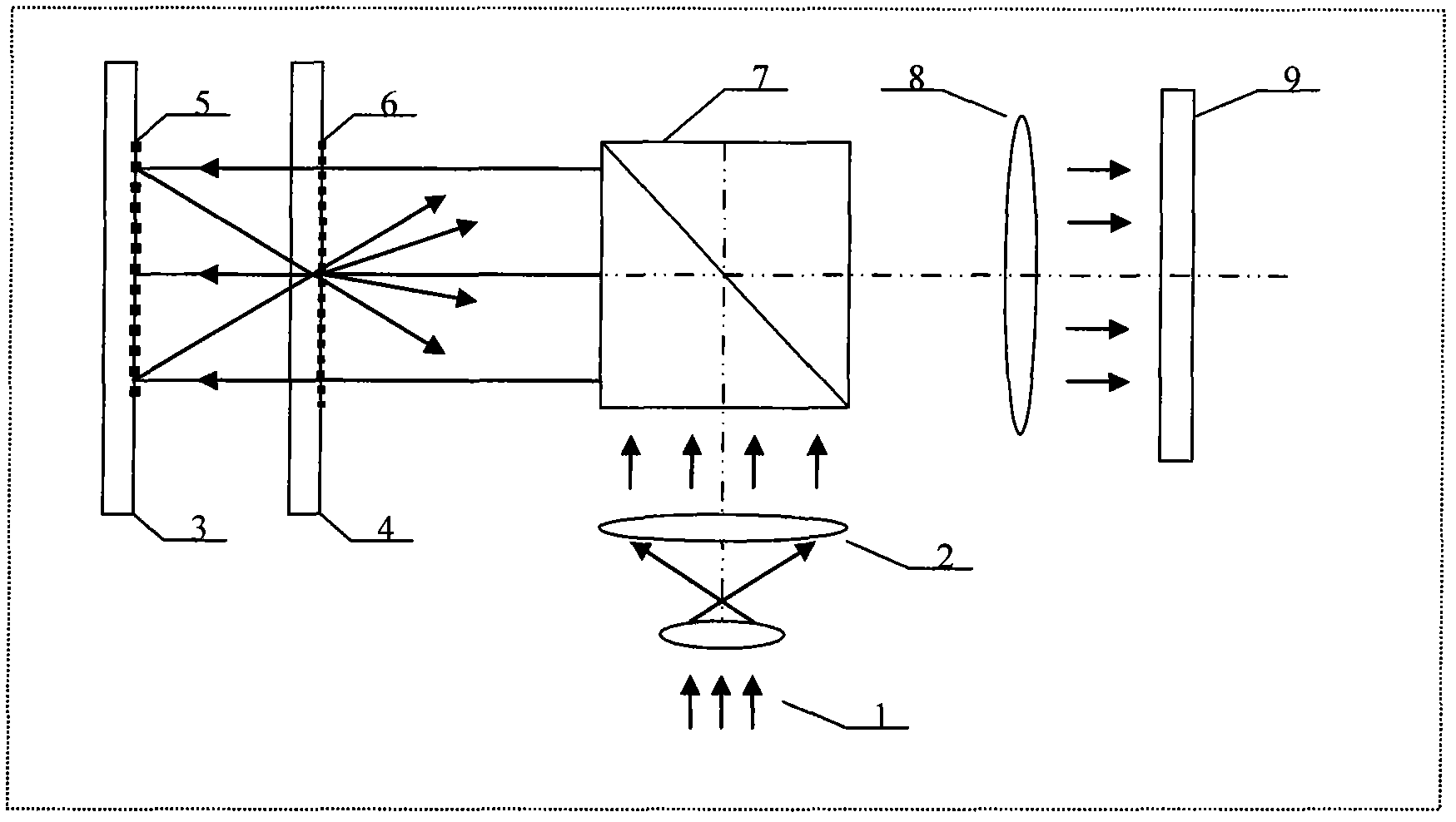
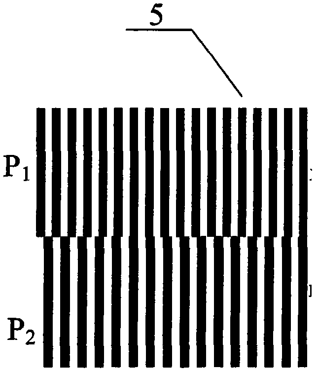
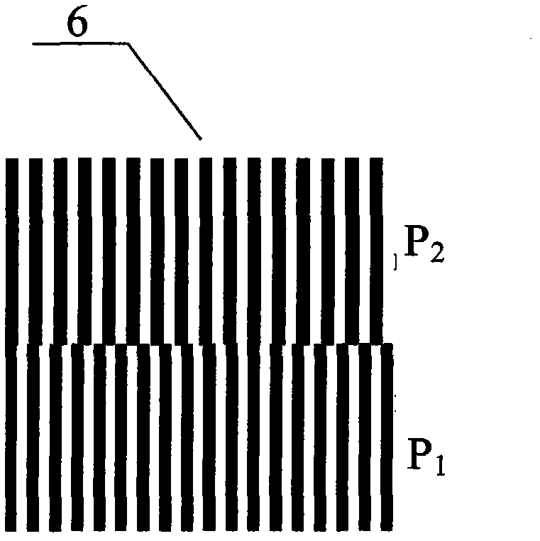
[0025] Such as figure 1 As shown, the optical path of the present invention is composed of a laser light source 1, a lens group 2, a mask 3, a silicon wafer 4, a mask grating 5, a silicon wafer grating 6, a beam splitter 7, an objective lens 8, and a CCD image detector 9. The laser light source 1 forms uniform collimated parallel light after passing through the lens group 2, and passes through the silicon wafer grating 6 on the silicon wafer 4 and the mask grating 5 on the mask 3. The periods of the two gratings are close, and the gap size It overlaps from 100nm to 200μm, so that multiple diffractions occur, and a certain two beams of diffracted light of the same level from two gratings interfere and superimpose, forming Moiré interference fringes whose period is enlarged relative to the original grating on the surface of the silicon wafer grating. Then pass through the beam splitter 7, and then pass through the objective lens 8 with a magnification of 8× to be imaged on the C...
PUM
 Abstract
Description
Claims
Application Information
 - R&D Engineer
- R&D Manager
- IP Professional
- Industry Leading Data Capabilities
- Powerful AI technology
- Patent DNA Extraction
Browse by: Latest US Patents, China's latest patents, Technical Efficacy Thesaurus, Application Domain, Technology Topic.
© 2024 PatSnap. All rights reserved.Legal|Privacy policy|Modern Slavery Act Transparency Statement|Sitemap