

Low-voltage low-power band gap reference voltage source implemented by MOS device
A technology of MOS devices and reference voltage sources, which is applied in the direction of instruments, electric variable adjustment, control/regulation systems, etc., can solve the problems of large circuit area, high static power consumption, and the minimum working voltage of reference sources cannot be reduced to a very low level. Achieve the effect of low static power consumption and low temperature drift coefficient
Active Publication Date: 2011-06-15
TSINGHUA UNIV
View PDF0 Cites 19 Cited by
- Summary
- Abstract
- Description
- Claims
- Application Information
AI Technical Summary
Problems solved by technology
1. Due to the existence of the amplifier, its static power consumption is high
2. Due to the need to use bipolar transistors, the area occupied by the circuit is generally relatively large
3. Due to the limitation of the minimum operating voltage of the amplifier, the minimum operating voltage of the reference source cannot be reduced to a very low level
Method used
View moreImage
Smart ImageViewing Examples

Examples
Embodiment Construction
Login to View More PUM
 Abstract
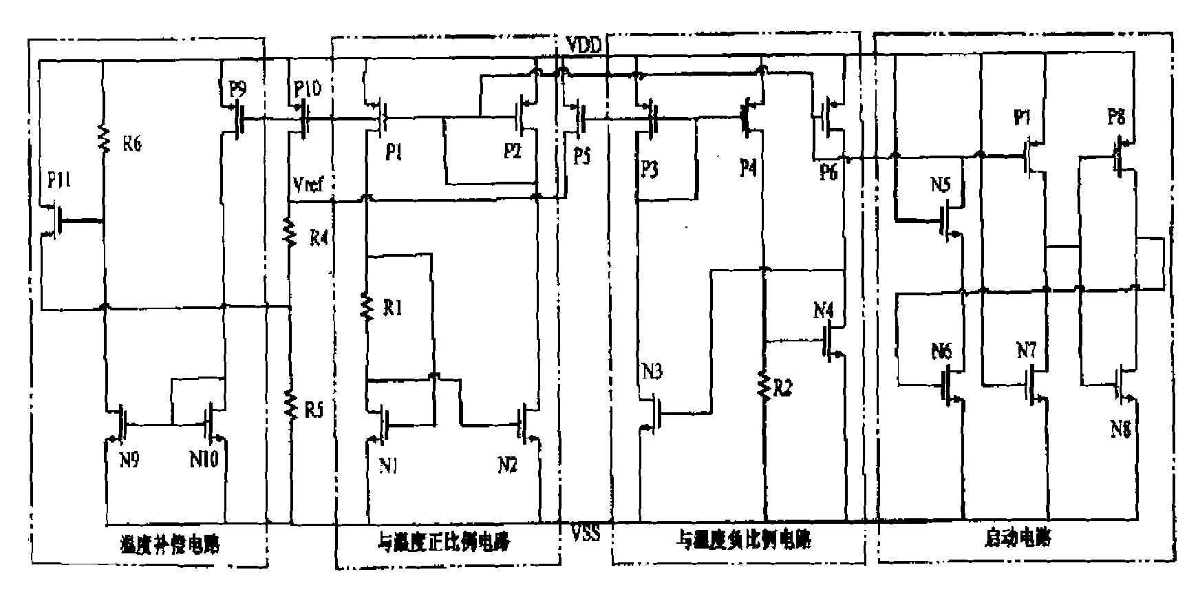
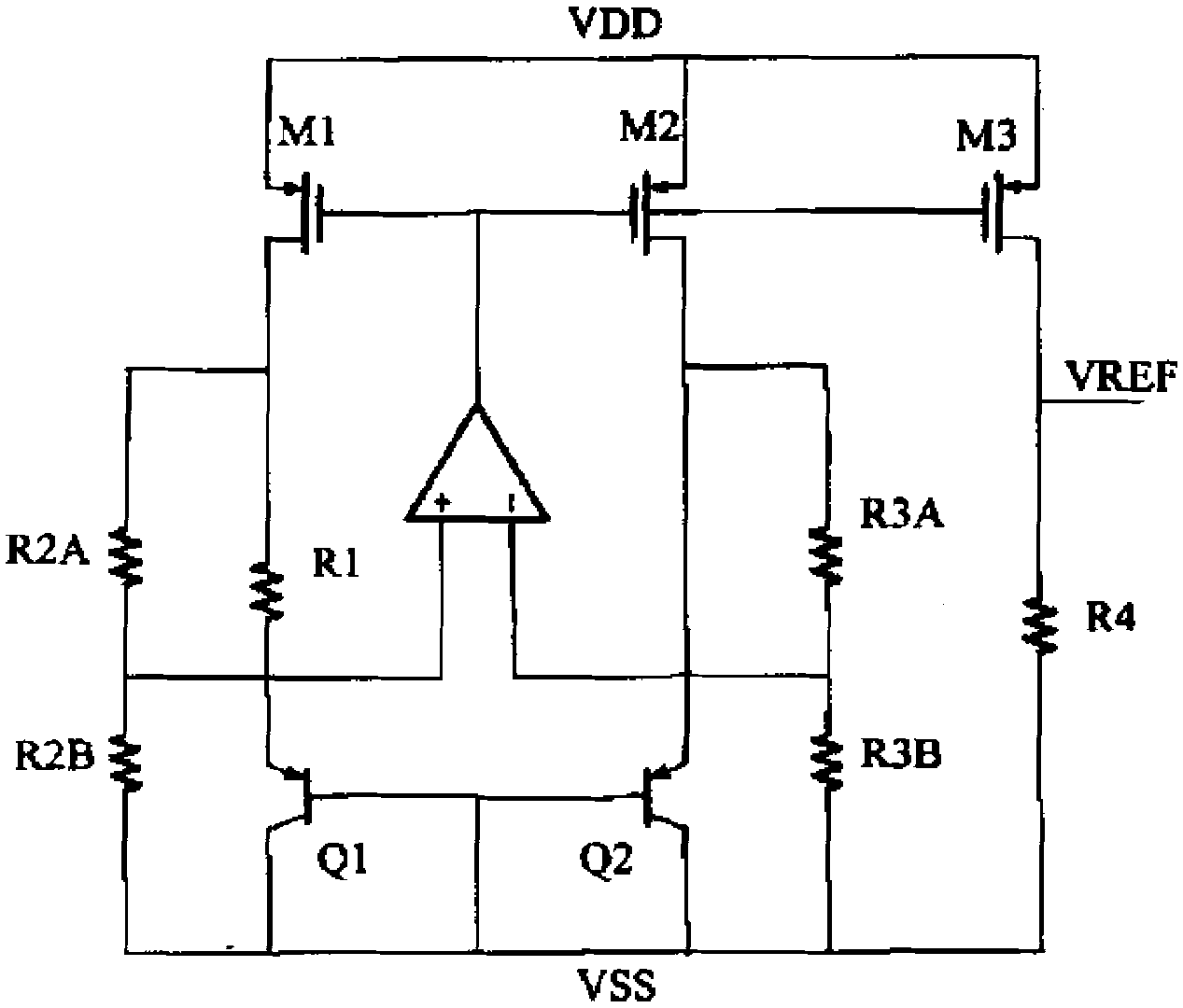
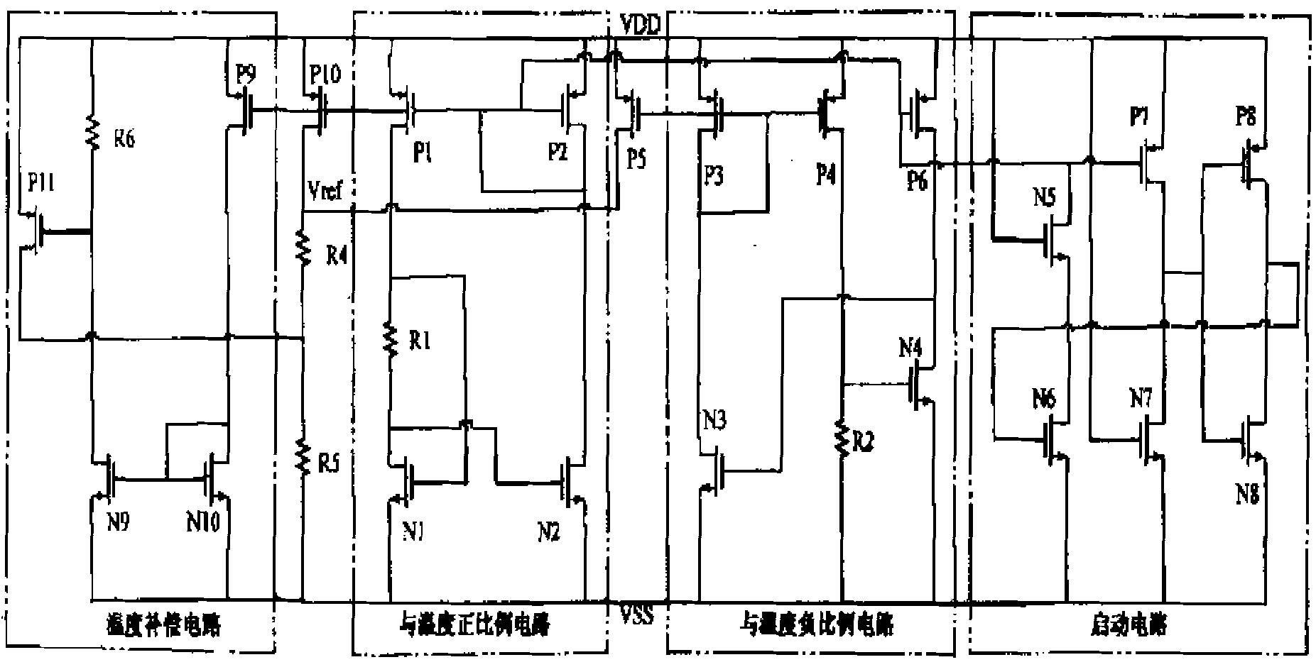
The invention discloses a low-voltage low-power band gap reference voltage source implemented by a MOS (Metal Oxide Semiconductor) device, which is implemented through the CMOS (Complementary Metal Oxide Semiconductor) technology, and comprises a circuit generating a current positively proportional to the temperature, a circuit generating a current inversely proportional to the temperature, a temperature secondary compensation circuit and a starting circuit; wherein the circuit generating the current positively proportional to the temperature obtains a voltage positively proportional to the temperature via a resistor, and simultaneously, the circuit generating the current inversely proportional to the temperature obtains a voltage inversely proportional to the temperature via the resistor, and the two voltages are added up to obtain a reference voltage unrelated to the temperature; additionally, the temperature secondary compensation circuit is used for compensating a high-order temperature coefficient of the reference voltage source so as to obtain a lower temperature-drift coefficient; the low-voltage low-power band gap reference voltage source provided by the invention has the advantages of low static power consumption, low temperature-drift coefficient, and capability of working in low-voltage environment and the like, and further improves the performance of the circuit.
Description
Low-voltage and low-power bandgap voltage reference realized by MOS devices technical field The invention belongs to the field of analog integrated circuit design. It particularly relates to a low-voltage low-power consumption bandgap reference voltage source. Background technique Since the 20th century, with the development of submicron and ultra-deep submicron technology and the increasing maturity of system chip technology, portable electronic products powered by batteries have achieved rapid development and rapid popularization. Since the development of battery technology is far behind the development of electronic systems, products ranging from heart pacemakers to hearing aids, mobile phones and various products have imposed strict restrictions on the supply voltage of electronic products. On the other hand, as the size of the device continues to shrink, the breakdown voltage of the process is also reduced, which also imposes strict restrictions on the power supply v...
Claims
Login to View More Application Information
Patent Timeline
 IPC IPC(8): G05F3/30
Inventor方华军赵晓许军梁仁荣王敬
OwnerTSINGHUA UNIV