Method for monitoring chip groove depth and wafer

A technology for trench depth monitoring and chip monitoring. It is used in mechanical depth measurement, semiconductor/solid-state device components, semiconductor devices, etc., and can solve problems such as poor accuracy and large chip trench depth delay.

Active Publication Date: 2011-06-15
FOUNDER MICROELECTRONICS INT
View PDF0 Cites 16 Cited by
  • Summary
  • Abstract
  • Description
  • Claims
  • Application Information

AI Technical Summary

Problems solved by technology

[0007] An embodiment of the present invention provides a method for monitoring the depth of a chip groove, so as to solve the problems of large time delay and poor accuracy in monitoring the depth of a chip groove in the prior art

Method used


Image

  • Method for monitoring chip groove depth and wafer
  • Method for monitoring chip groove depth and wafer
  • Method for monitoring chip groove depth and wafer

Examples


Embodiment Construction

[0023] Embodiments of the present invention will be described in detail below in conjunction with the accompanying drawings.

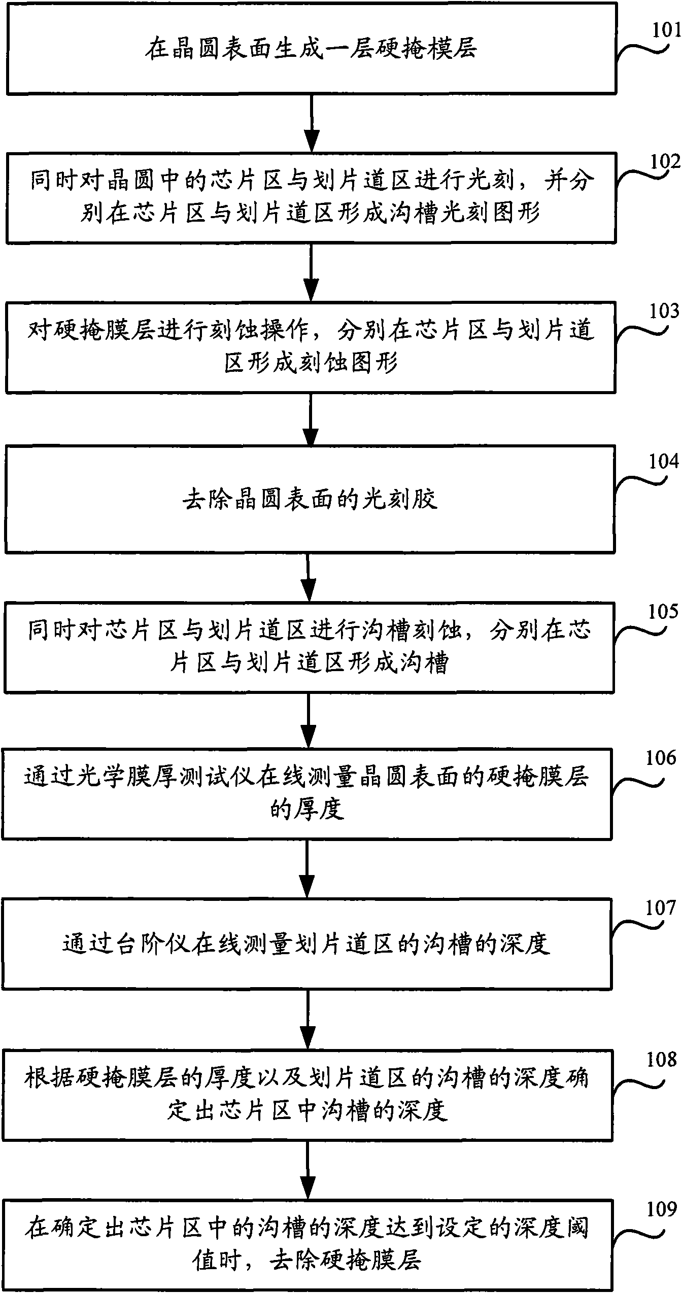
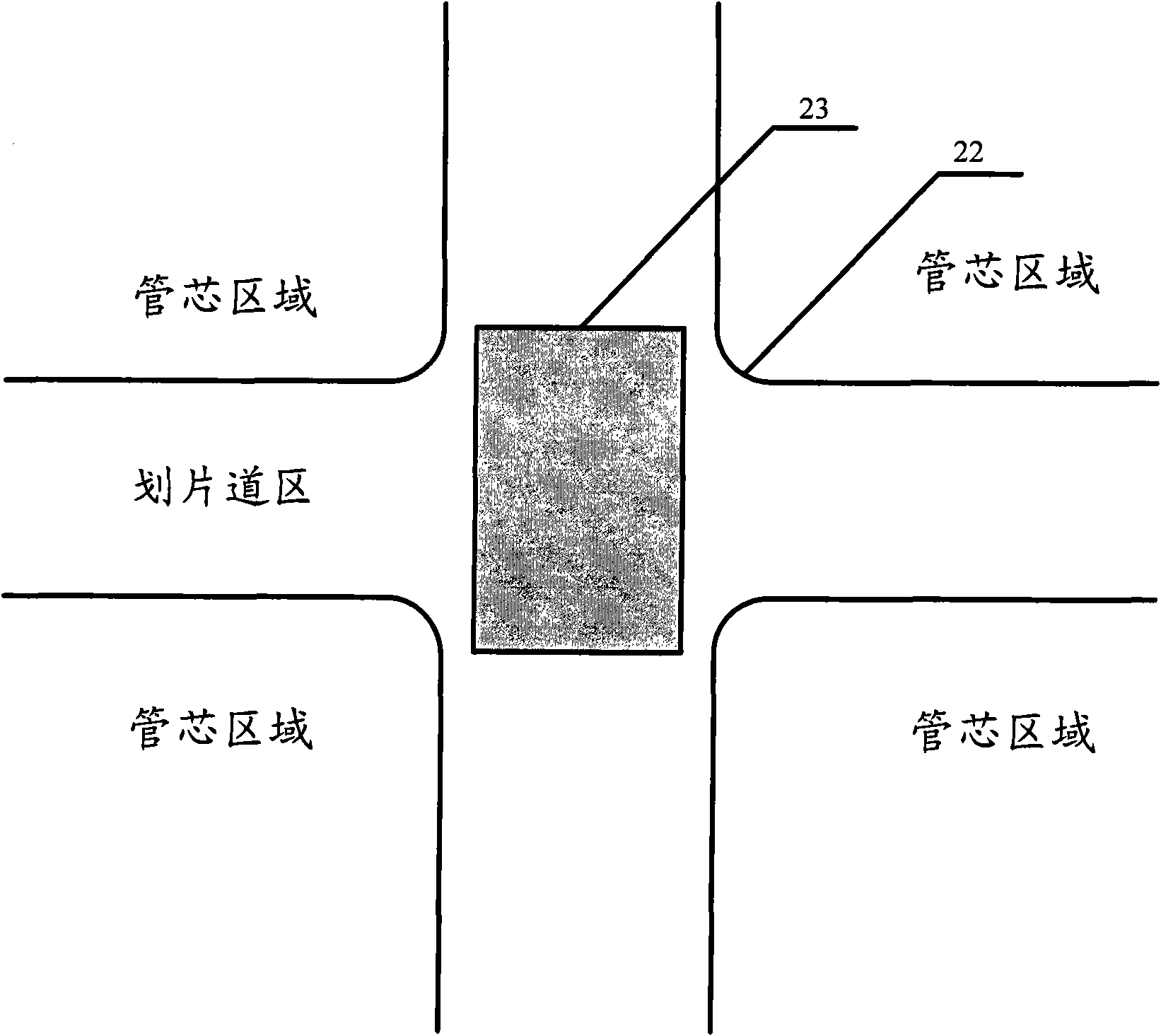
[0024] see figure 1 , is the flow chart of the method for realizing the real-time monitoring of the groove depth in the embodiment of the present invention. The module shaped as a cuboid (that is, the groove depth test module) is filled in the cross-staggered area of ​​the wafer surface in advance. The polarity of the module is consistent with the chip area. The polarity of the trench photoresist layer is the same, and during the photolithography process, the cuboid module is a photolithography open area; the process includes the following steps:

[0025] Step 101 , forming a protective film, such as a hard mask layer 31 , on the surface of the wafer 21 .

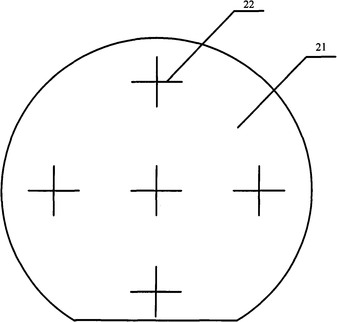
[0026] The structure of the wafer in this step is as follows Figure 2B As shown, is in the existing as Figure 2A All or part of the criss-cross region 22 of the wafer 21 shown is filled with t...


PUM


Abstract

The invention discloses a method for monitoring chip groove depth, which aims to solve the problems of longer time delay on monitoring of the chip groove depth and poor accuracy in the prior art. The method comprises the following steps of: generating a layer of protective film on the surface of a wafer; carrying out groove photoetching and corrosion on a chip area and a scribing channel area of the wafer, forming a first groove in the chip area, and forming a second groove used for detecting the depth of the first groove in the scribing channel area, wherein the polarity of a groove depth testing module is identical to the polarity of a groove photoetching layer in the chip area; measuring the depth d1 of the second groove by a step profiler; and monitoring the depth d of the first groove according to the d1 and the thickness d2 of the protective film. By adopting the technical scheme, the time delay on monitoring of the groove depth can be shortened, and the accuracy on controlling of the chip groove depth is improved.

Description

technical field [0001] The invention relates to the technical field of semiconductor device layout design, in particular to a method for monitoring the depth of a chip groove and a wafer. Background technique [0002] Source-drain breakdown voltage Bvdss and source-drain on-resistance Rdson are key parameters of low-voltage trench DMOS (Double-diffused Metal Oxide Semiconductor) devices. These two parameters are relatively sensitive to each other. Under normal circumstances, the expected value of Bvdss is 20 volts to 100 volts, and the expected value of Rdson is less than a dozen milliohms. Since the values ​​of Bvdss and Rdson are related to the groove depth, different groove depths may determine different values. Bvdss and Rdson, therefore, it is particularly important to precisely control the depth of the trench during the dry etching trench process. [0003] At present, the commonly designed DMOS trench photolithography layer layout only needs to have a trench pattern i...

Claims


Application Information

Patent Timeline
Patent Type & Authority Applications(China)
IPC IPC(8): H01L21/00H01L23/544G01B5/18
Inventor 陈勇方绍明张立荣王新强曾永祥
Owner FOUNDER MICROELECTRONICS INT
Why Eureka
Try Eureka