Light emitting diode with oxide nano array structure and preparation method thereof

A technology of light-emitting diodes and nano-arrays, which is applied to electrical components, circuits, semiconductor devices, etc., can solve problems such as difficulty in repairing, and achieve the effects of reducing the current concentration effect, improving the light output rate, and reducing the effect of total reflection.

Inactive Publication Date: 2011-06-15
AQUALITE CO LTD
View PDF3 Cites 10 Cited by
  • Summary
  • Abstract
  • Description
  • Claims
  • Application Information

AI Technical Summary

Problems solved by technology

So far, there have been many reports on plasma etching damage

Method used


Image

  • Light emitting diode with oxide nano array structure and preparation method thereof
  • Light emitting diode with oxide nano array structure and preparation method thereof
  • Light emitting diode with oxide nano array structure and preparation method thereof

Examples


Embodiment Construction

[0061] The principles and features of the present invention are described below in conjunction with the accompanying drawings, and the examples given are only used to explain the present invention, and are not intended to limit the scope of the present invention.

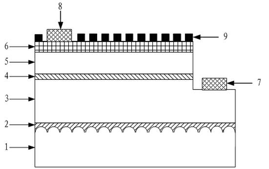
[0062] Such as figure 1 As shown, in the first implementation of the light-emitting diode of the present invention, the light-emitting diode includes a substrate 1, a buffer layer 2, an N-type layer 3, an active layer 4, a P-type layer 5, and a layer disposed on the P-type layer in sequence. Transparent conductive layer 6 on 5, N-type layer 3 is provided with N-electrode 7, P-type layer 5 is provided with P-electrode 8, N-type layer 3 is an N-type GaN layer, and P-type layer 5 is a P-type GaN layer. The surface of the transparent conductive layer 6 is covered with oxide particles 9 distributed in an array. Wherein, the material of the oxide particles 9 is Al 2 o 3 、 Ta 2 o 5 、TiO 2 , ZnO, ZrO 2 One or a combi...


PUM

PropertyMeasurementUnit
Heightaaaaaaaaaa

Abstract

The invention relates to a light emitting diode (LED) with an oxide nano array structure and a preparation method thereof. The LED comprises a transparent conductive layer deposited on the surface of the LED, and oxide granules covered on the surface of the transparent conductive layer or embedded in the transparent conductive layer and distributed in array. The preparation method for the LED comprises steps of spin coating, stamping, ultraviolet (UV) irradiation, stripping, reactive ion etching (RIE), deposition and lift-off, and can also comprise an etching step between the RIE and deposition steps. The oxide granule structure distributed in array in the LED can cause scattering of light and destroy the light of original total internal reflection to allow more photons to escape from the LED so as to reduce the total reflection influence of the LED and improve the light emitting rate of the LED. The preparation method does not refer to plasma etching of an active layer and a p-type GaN at the same time of improving the light extraction efficiency of the LED, so plasma damage is not caused to affect the electric performance of the LED.

Description

technical field [0001] The invention relates to a light-emitting diode and a preparation method thereof, more specifically, to a light-emitting diode with an oxide nano-array structure and a preparation method thereof. Background technique [0002] Light Emitting Diode (LED, Light Emitting Diode) has the characteristics of energy saving, environmental protection and long life, and is widely used in the fields of backlight, traffic light and lighting. It is expected that LED will replace incandescent lamps and fluorescent lamps in the future and become a new generation of lighting sources. However, the promotion of the LED lighting market is still restricted by two aspects: one is that its luminous efficiency is not high, generally 100 lm / W, which is equivalent to the efficiency of fluorescent lamps; 5 to 10 times. The former is the key to solving the problem. [0003] The luminous efficiency of LED is limited by the external quantum efficiency, and the external quantum ef...

Claims


Application Information

Patent Timeline
IPC IPC(8): H01L33/44H01L33/00
Inventor 王汉华项艺杨新民靳彩霞董志江
Owner AQUALITE CO LTD
Why Eureka
Try Eureka