
Clock signal generating circuit

A clock signal and generation circuit technology, which is applied in the direction of electric pulse generator circuit, electric pulse generation, pulse generation, etc., can solve the problem of high power consumption of clock signal circuit, uncontrollable current of crystal oscillator unit and clock shaping circuit, and increase of chip power. Consumption and other issues, to achieve the effect of reducing power consumption

Inactive Publication Date: 2011-06-15
VIMICRO CORP
View PDF4 Cites 12 Cited by
  • Summary
  • Abstract
  • Description
  • Claims
  • Application Information

AI Technical Summary

Problems solved by technology

[0005] However, in the existing clock signal generating circuit, since the original clock signal output by the crystal oscillator unit is directly shaped by the inverter of the clock shaping circuit, the current of the crystal oscillator unit and the clock shaping circuit cannot be controlled, and the entire clock signal generating circuit The power consumption is relatively large, and it will also increase the power consumption of the chip for the entire chip

Method used


Image

  • Clock signal generating circuit
  • Clock signal generating circuit
  • Clock signal generating circuit

Examples


Embodiment Construction

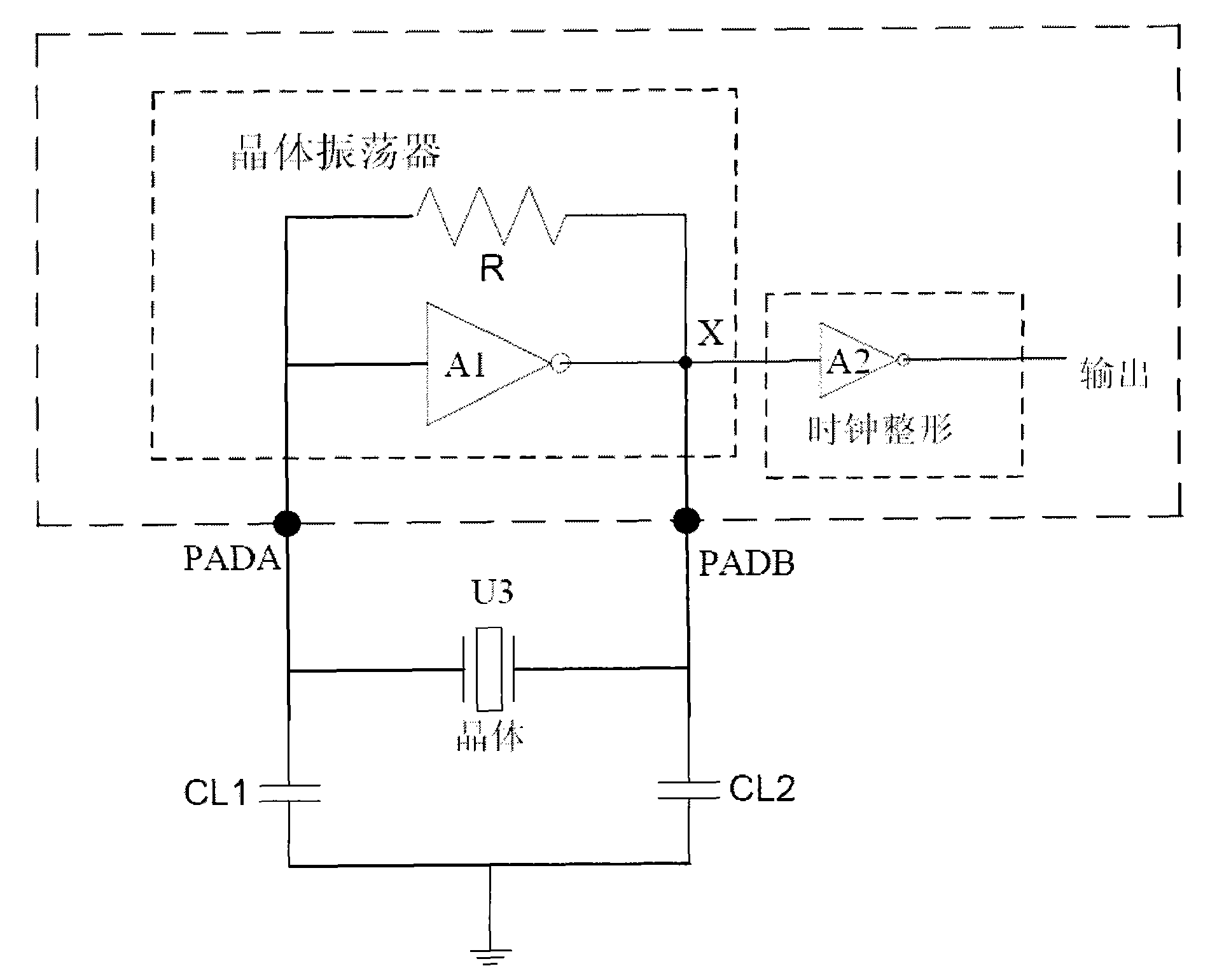
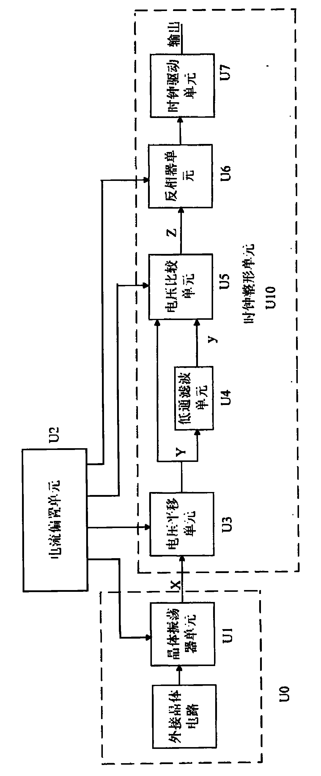
[0025] see figure 2 As shown, it shows the structural block diagram of the clock signal generating circuit of the present invention. The clock signal generation circuit in the present invention includes a crystal oscillator unit U0, a current bias unit U2 and a clock shaping unit U10.

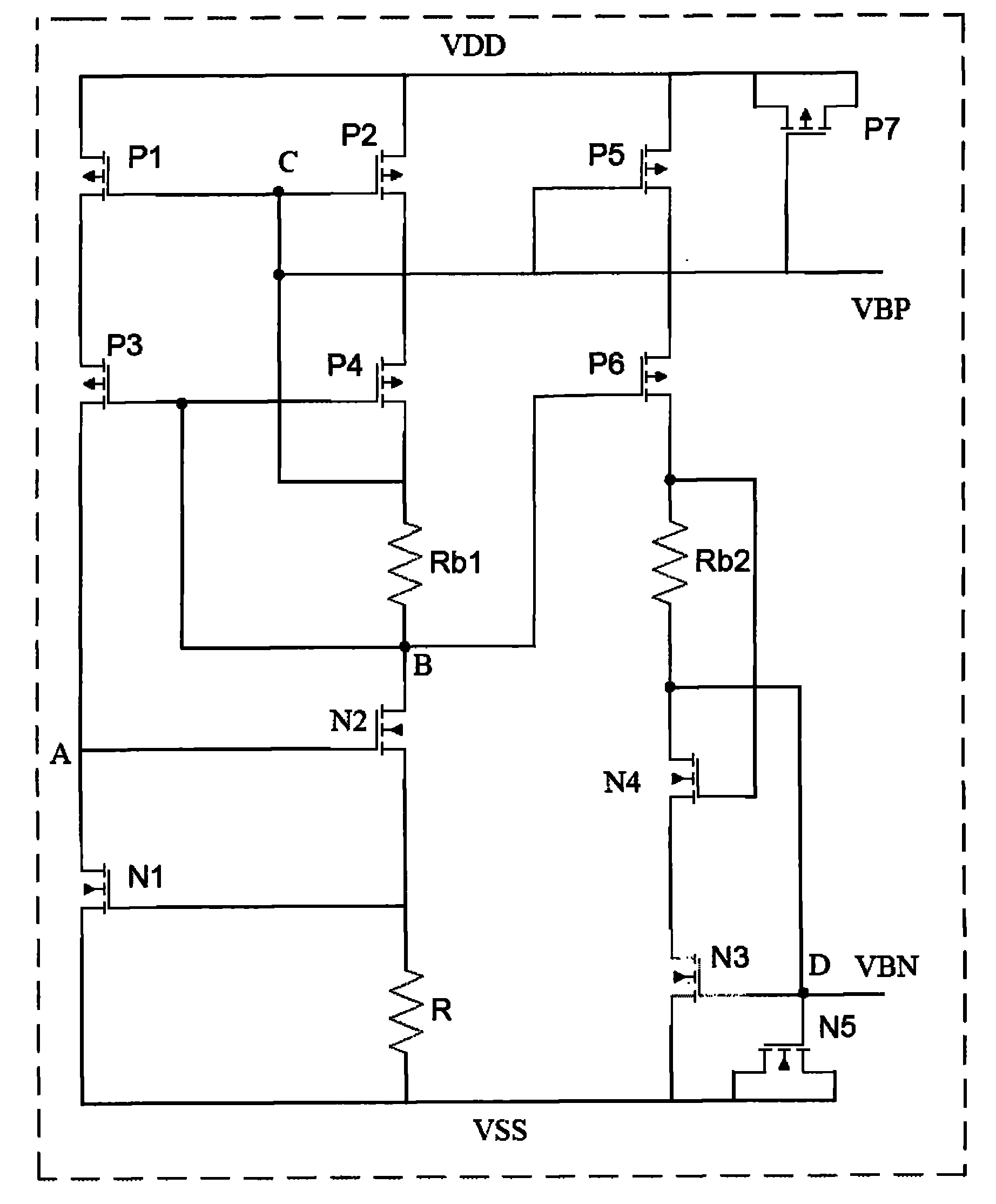
[0026] The crystal oscillation unit generates an original clock signal X, and then inputs the original clock signal X to the clock shaping unit U10 for shaping, and finally outputs a standard clock signal with a standard square wave waveform. During the entire clock signal generation and shaping process, the current bias unit U2 generates a reference current (or bias current), and the crystal oscillator unit and the clock shaping unit mirror the reference current of the current bias unit, and use this mirror current as The working current of each unit is controlled and adjusted by the reference circuit of the current bias unit, which can control and adjust the current of the whole circuit, so...


PUM


Abstract

The invention provides a clock signal generating circuit which comprises a crystal oscillation unit and a clock shaping unit, wherein the crystal oscillation unit generates an initial clock signal, and the clock shaping unit is used for shaping the initial clock signal and then outputting a standard clock signal. The clock signal generating circuit also comprises a current bias unit connected with the crystal oscillation unit and the clock shaping unit, wherein the crystal oscillation unit and the clock shaping unit mirror the bias current of the current bias unit, and the mirror current is used as a working current, so that the currents of the crystal oscillation unit and the clock shaping unit can be controlled and regulated by controlling the current of the current bias unit.

Description

【Technical field】 [0001] The invention relates to the field of electronic circuits, in particular to a clock signal generation circuit with improved power consumption. 【Background technique】 [0002] In the field of microelectronics, especially in various electronic chips, it is often necessary to use standard clock signals of square wave waveforms with amplitudes of 0 and 1 as control signals for other circuits. In order to provide this standard clock signal, it is usually necessary to design a clock signal generating circuit. Such as figure 1 As shown, it shows the clock generation circuit of the commonly used CMOS chip at present, which includes a crystal oscillation unit composed of an external crystal U3, load capacitors CL1, CL2, and an internal crystal oscillator, and a clock shaping circuit. [0003] The external crystal U3 and the two load capacitors CL1 and CL2 are connected in series, and the connected ends of the two capacitors CL1 and CL2 are grounded. The tw...

Claims


Application Information

Patent Timeline
Patent Type & Authority Applications(China)
IPC IPC(8): H03K3/012H03K3/023
Inventor 龚川
Owner VIMICRO CORP
Learn More