
Pad structure and manufacturing method thereof

A gold layer and nanotechnology, applied in the direction of electrical connection of printed components, formation of electrical connections of printed components, semiconductor/solid-state device manufacturing, etc., can solve problems such as insufficient wear resistance of the nickel-gold layer surface

Inactive Publication Date: 2011-06-15
ADVANCE MATERIALS CORP
View PDF0 Cites 4 Cited by
  • Summary
  • Abstract
  • Description
  • Claims
  • Application Information

AI Technical Summary

Problems solved by technology

However, the surface wear resistance of the nickel-gold layer formed by the previous technology is obviously insufficient, so further improvement and improvement are still needed

Method used


Image

  • Pad structure and manufacturing method thereof
  • Pad structure and manufacturing method thereof
  • Pad structure and manufacturing method thereof

Examples


Embodiment Construction

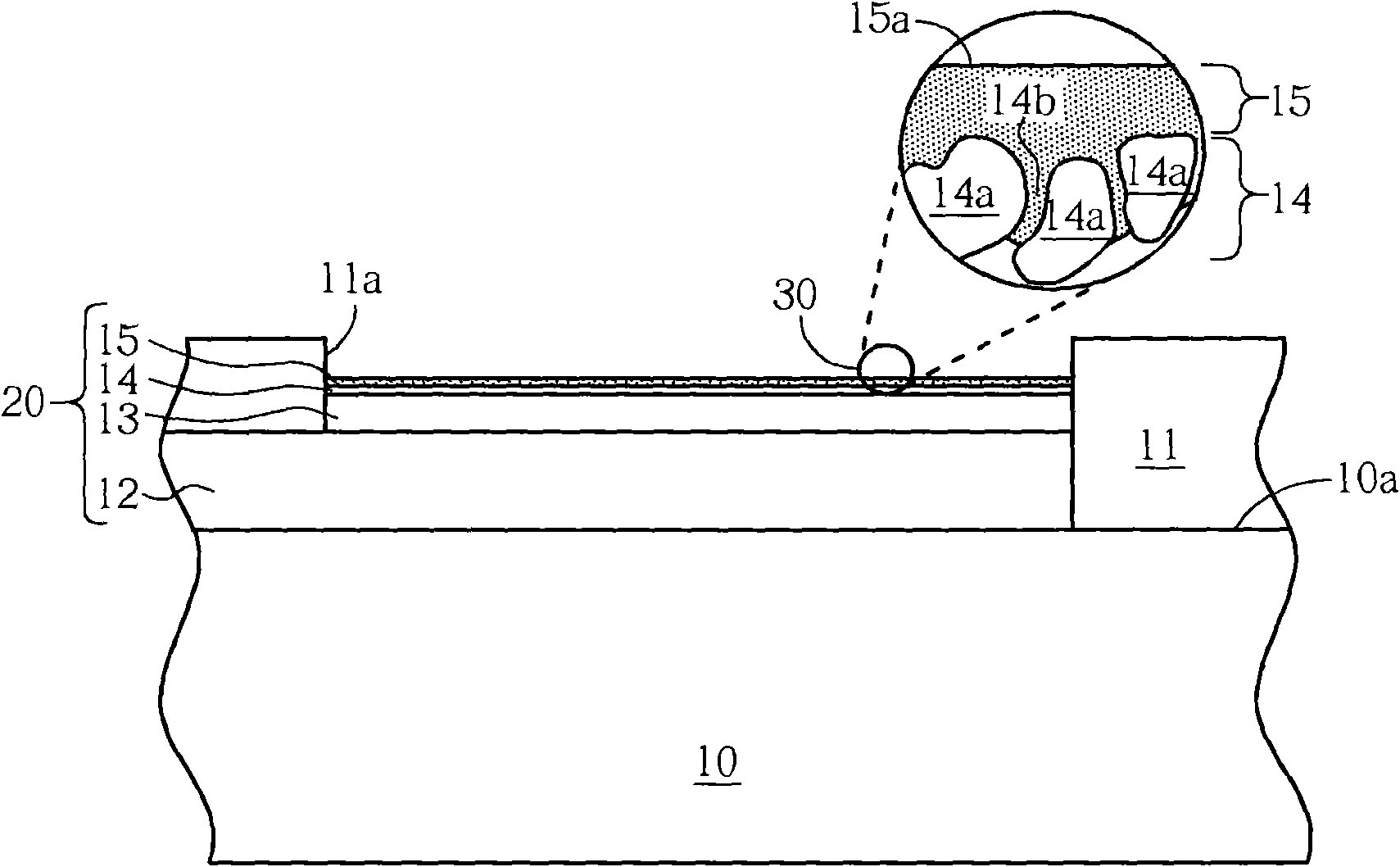
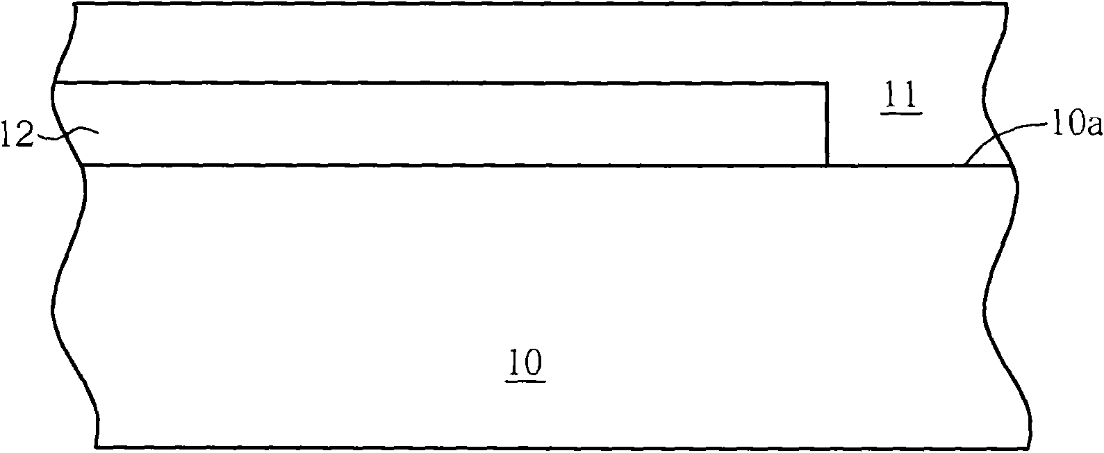
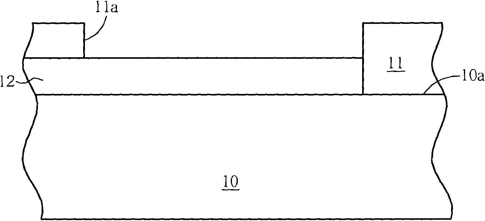
[0037] Throughout the following specification, "pad" or "pad structure" broadly refers to a bonding pad or a contact pad structure, where the bonding pad can be a wire-bond finger or a solder bond pad. ), etc., and the contact pads may include electrical contact gold fingers on the substrate, for example, external contact fingers of a DRAM, or input / output pads (input / output pads) on an integrated circuit chip, and the like. Although, in the following preferred embodiments, the exposed electrical contact or pad structure on the circuit board or package substrate is used as an example for illustration, the present invention is not limited to these application fields, but should be based on the attached The scope of the invention is defined by the claims.

[0038] Please refer to figure 1 , which is a schematic cross-sectional view of a pad structure according to a preferred embodiment of the present invention. Such as figure 1 As shown, according to the preferred embodiment ...


PUM

PropertyMeasurementUnit
thicknessaaaaaaaaaa
thicknessaaaaaaaaaa
thicknessaaaaaaaaaa

Abstract

The invention discloses a pad structure, which comprises a copper circuit pattern arranged on a substrate, a gold layer superposed on the copper circuit pattern and a nanometer film coating superposed on the gold layer.

Description

technical field [0001] The present invention relates to a novel pad structure, in particular to an exposed electrical contact or pad structure on a circuit board or a package substrate and a manufacturing method thereof. The invention also has the advantages of low cost, wear resistance, scratch resistance and corrosion resistance. Background technique [0002] In the manufacturing process of circuit board or package substrate, in addition to forming a fine copper wire pattern, it will eventually be on the exposed electrical connection points, such as wire-bond fingers. finger), solder bond pad (solder bond pad) and other bonding pads or contact pads, and a nickel-gold (Ni / Au) layer is also plated to ensure a stable and reliable electrical connection between the circuit board or substrate and the chip. . At the same time, the nickel-gold layer also has the function of preventing the oxidation of copper wires. [0003] Those skilled in the art can understand that the curre...

Claims


Application Information

Patent Timeline
Patent Type & Authority Applications(China)
IPC IPC(8): H05K1/11H05K3/40H05K3/24H01L23/48H01L21/48
CPCH01L2924/0002
Inventor 颜立盛
Owner ADVANCE MATERIALS CORP
Learn More