Pixel structure and display panel

A pixel structure and display panel technology, applied in static indicators, optics, instruments, etc., can solve problems such as voltage drop, unfavorable signal transmission, etc., and achieve the effect of increasing update rate

Inactive Publication Date: 2013-07-10
AU OPTRONICS CORP
View PDF2 Cites 0 Cited by
  • Summary
  • Abstract
  • Description
  • Claims
  • Application Information

AI Technical Summary

Problems solved by technology

At this time, the impedance of the scan line and the data line is bound to increase, which is not conducive to signal transmission.
For example, the voltage transmitted by the scan line or data line tends to decrease gradually due to the increase of impedance

Method used


Image

  • Pixel structure and display panel
  • Pixel structure and display panel
  • Pixel structure and display panel

Examples


Embodiment Construction

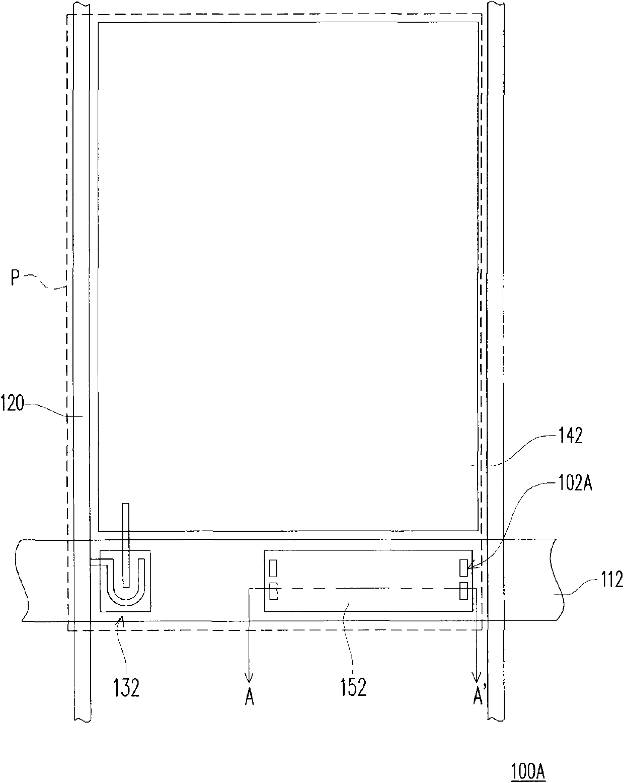
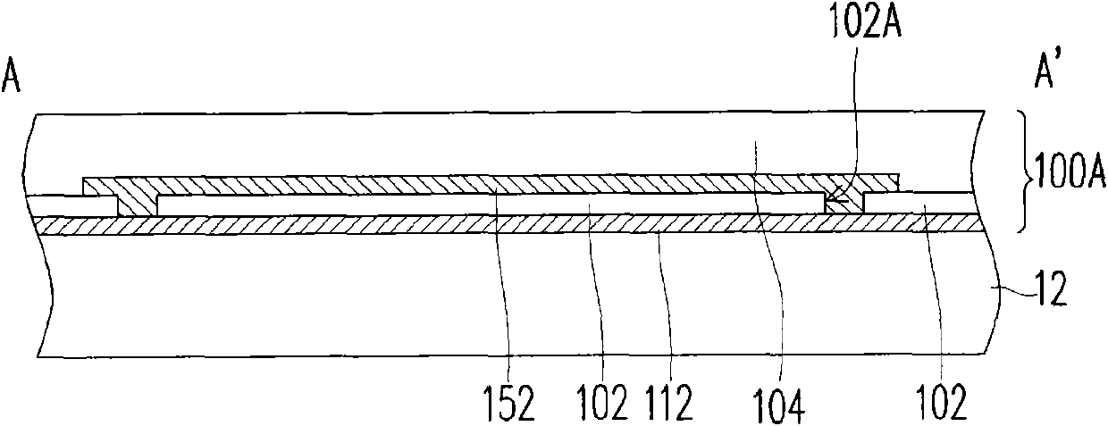
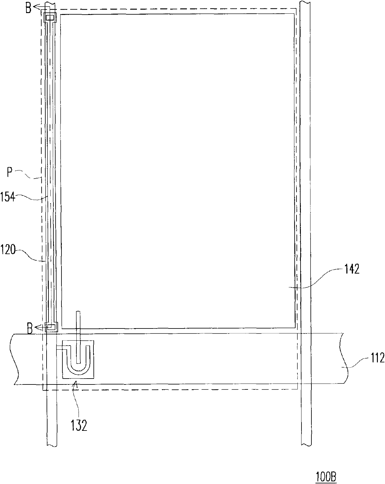
[0041] figure 1 It is a schematic top view of the pixel structure according to the first embodiment of the present invention, and figure 2 for along figure 1 The cross-sectional schematic diagram drawn by the section line A-A'. Please refer to figure 1 and figure 2 The pixel structure 100A includes a first scan line 112 , a data line 120 , a first active device 132 , a first pixel electrode 142 and a first conductive pattern 152 . The first active device 132 is connected to the first scan line 112 and the data line 120 . The first pixel electrode 142 is electrically connected to the data line 120 through the first active device 132 . The first conductive pattern 152 is located above the first scan line 112 and connected in parallel to the first scan line 112 .

[0042] Depend on figure 2 It can be seen that the pixel structure 100A is disposed on the substrate 12 , and the pixel structure 100A further includes a gate insulating layer 102 and a protection layer 104 . ...


PUM


Abstract

The invention provides a pixel structure and a display panel. The pixel structure comprises a first scanning line, a data wire, a first active element, a first pixel electrode and a first conductive pattern, wherein the first active element is connected with the first scanning line and the data wire; the first pixel electrode is electrically connected with the data wire through the first active element; and the first conductive pattern is positioned above the first scanning line and connected in parallel with the first scanning line.

Description

technical field [0001] The present invention relates to a pixel structure and a display panel, and in particular to a pixel structure and a display panel with good signal transmission. Background technique [0002] The rapid progress of the multimedia society is largely due to the rapid progress of semiconductor devices and display devices. As far as displays are concerned, liquid crystal displays (Liquid Crystal Displays, LCDs) with superior characteristics such as high image quality, good space utilization efficiency, low power consumption, and no radiation have gradually become the mainstream of the market. Generally speaking, a liquid crystal display includes a liquid crystal display panel (LCD panel) and a backlight module for providing a surface light source. composition. [0003] The thin film transistor array substrate is mainly composed of a plurality of scanning lines, a plurality of data lines and a plurality of pixel structures arranged on the substrate. Each ...

Claims


Application Information

Patent Timeline
Patent Type & Authority Patents(China)
IPC IPC(8): G02F1/1362H01L27/02H01L23/52G02F1/1343G09G3/36
Inventor 何昇儒曹正翰邱钟毅
Owner AU OPTRONICS CORP
Why Eureka
Try Eureka