Active matrix substrate and manufacturing method thereof

An active matrix and substrate technology, applied in the field of optical sensor structure and its manufacturing, can solve the problems of low detection sensitivity of optical sensors and the like

Active Publication Date: 2011-07-06
BOE TECH GRP CO LTD +1
View PDF0 Cites 7 Cited by
  • Summary
  • Abstract
  • Description
  • Claims
  • Application Information

AI Technical Summary

Problems solved by technology

[0004] The purpose of the present invention is to provide an active matrix substrate and its manufacturing method, which can effectively solve the defects of low detection sensitivity of existing optical sensors and the need for additional circuit structures to cooperate with optical sensors for detection.

Method used


Image

  • Active matrix substrate and manufacturing method thereof
  • Active matrix substrate and manufacturing method thereof
  • Active matrix substrate and manufacturing method thereof

Examples


Embodiment Construction

[0056] The technical solutions of the present invention will be described in further detail below with reference to the accompanying drawings and embodiments.

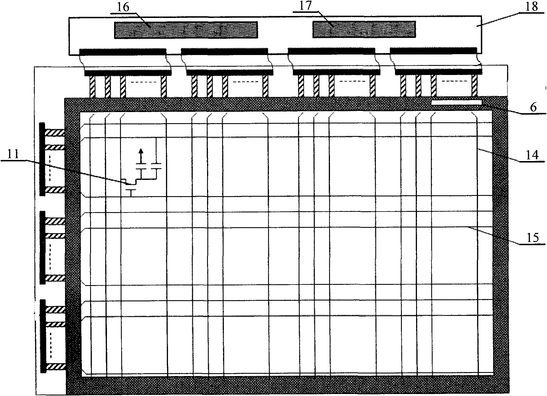
[0057] figure 1 It is a structural schematic diagram of the active matrix substrate of the liquid crystal display device of the present invention. Such as figure 1 As shown, in the display area on the active matrix substrate, vertical lines (data lines) 14 and horizontal lines (gate lines) 15 are arranged vertically and intersecting each other. The gate lines 15 and data lines 14 define each pixel area, and form pixel electrodes in the pixel area. and a thin film transistor (TFT) 11 . A photosensor 6 having a triode structure is formed on the substrate. The peripheral circuits on the active matrix substrate are connected to the external circuit board 18 through a flexible printed circuit (FPC). The external circuit board 18 has a first circuit 16 that provides drive control signals for the data line 14 and the gate...


PUM


Abstract

The invention relates to an active matrix substrate and manufacturing method thereof. The active matrix substrate comprises a display region and a non-display region, wherein the display region comprising grid lines and data lines formed on the substrate, and each pixel region defined by the grid lines and the data lines, wherein a pixel electrode and a film transistor are formed in the pixel region; and an optical sensor with an audion structure is formed on the substrate. The active matrix substrate is provided with the optical sensor with the audion structure so that the optical sensitive current generated by the external light is amplified in the optical sensor, the output signal of the optical sensor is increased and the flexibility of the optical sensor for detecting the external light is improved.

Description

technical field [0001] The invention relates to a light sensor structure of a liquid crystal display and a manufacturing method thereof, in particular to an active matrix substrate with a light sensor and a manufacturing method thereof. Background technique [0002] In recent years, the development of liquid crystal display devices has been directed toward light weight, thin profile, and low power consumption. In terms of reducing power consumption, the purpose of reducing power consumption can be achieved by preparing or integrating a photosensor in the liquid crystal display device, and adjusting the intensity of light from the backlight according to the intensity of ambient light detected by the photosensor. [0003] The light sensor that detects the intensity of ambient light can use a light sensor such as a photodiode or a phototransistor, and the light sensor is installed on the liquid crystal display panel in the form of a discrete component. In order to reduce the m...

Claims


Application Information

Patent Timeline
Patent Type & Authority Applications(China)
IPC IPC(8): G02F1/1362G02F1/1333H01L27/144H01L31/11H01L21/82H01L31/18H01L31/20
CPCY02P70/50
Inventor 惠官宝
Owner BOE TECH GRP CO LTD
Why Eureka
Try Eureka