Communication device and circuit board structure thereof

A technology for communication devices and circuit boards, applied in printed circuit components, electrical components, magnetic field/electric field shielding, etc., can solve problems such as noise interference, and achieve the effect of reducing the overall volume

Active Publication Date: 2012-09-19
ACER INC
View PDF0 Cites 0 Cited by
  • Summary
  • Abstract
  • Description
  • Claims
  • Application Information

AI Technical Summary

Problems solved by technology

[0005] The technical problem to be solved by the present invention is to make up for the above-mentioned deficiencies in the prior art, and propose a communication device and its circuit board structure, so as to solve the problem of noise interference between multiple circuits in the existing circuit board when they share a metal shielding layer. The problem

Method used


Image

  • Communication device and circuit board structure thereof
  • Communication device and circuit board structure thereof
  • Communication device and circuit board structure thereof

Examples


Embodiment Construction

[0042] The present invention will be described in further detail below in combination with specific embodiments and with reference to the accompanying drawings.

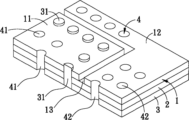
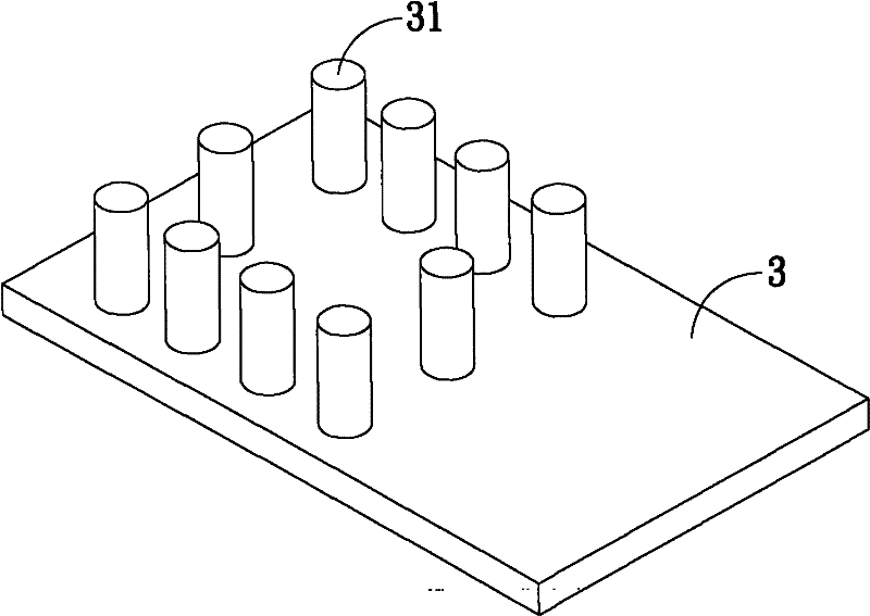
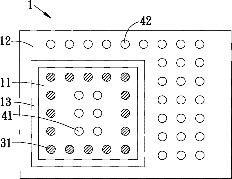
[0043] Such as figure 1 Shown is a partial cross-sectional schematic diagram of the circuit board structure of this embodiment. figure 1 Among them, the circuit board structure includes a circuit layer 1 , an insulating layer 2 and a grounding layer 3 , wherein the insulating layer 2 is disposed below the circuit layer 1 , and the grounding layer 3 is disposed below the insulating layer 2 . The circuit board structure includes a plurality of openings 4 , and each opening 4 has a conductive structure, so that the circuit layer 1 can be electrically connected to the ground layer 3 through the openings 4 . Wherein, the circuit layer 1 may be one of lead, tin, silver, copper, gold, bismuth, antimony, zinc, nickel, zirconium, magnesium, indium, tellurium, gallium, palladium and an alloy composed of the aforementioned met...


PUM


Abstract

The invention discloses a communication device which comprises a circuit board, a first metal shielding structure, a radio frequency circuit and a fundamental frequency circuit, wherein the circuit board comprises a circuit layer, an insulation layer and a grounding layer; the insulation layer is arranged below the circuit layer, the grounding layer is arranged below the insulation layer, and thegrounding layer upwards passes through the insulation layer and is provided with an isolated body in an extending way so as to isolate a first circuit area from a second circuit area; the first circuit area and the grounding end of the second circuit area are electrically connected with the grounding layer, and a gap is arranged between the first circuit area and the isolated body; and the radio frequency circuit is arranged on the first circuit area, the foundational frequency circuit is arranged on the second circuit area, and the first metal shielding structure is arranged above the circuit board structure and electrically connected with the isolated body so that the first circuit area and the second circuit area are not easy to interfer by respective noise.

Description

technical field [0001] The invention relates to a communication device and its circuit board structure, in particular to a communication device and its circuit board structure in which a plurality of circuits are not easily interfered by mutual noise. Background technique [0002] In the prior art, when a plurality of different circuits are arranged on a circuit board, each part of the circuit has its own metal shielding layer, and the ground terminal of each circuit is connected to its own metal shielding layer to enhance noise The effect of isolation. In addition, under the known metal shielding layer, dense metal fences are inserted into the circuit board to enhance the shielding effect between the circuits. [0003] However, with the continuous advancement of science and technology, the requirements for electronic devices are becoming more and more refined, both small in size and strong in functionality. More often, there is not enough space in the electronic device fo...

Claims


Application Information

Patent Timeline
Patent Type & Authority Patents(China)
IPC IPC(8): H05K1/02H05K1/11H05K9/00
Inventor 许振贤
Owner ACER INC
Why Eureka
Try Eureka