Silicon chip edge protection device and application method thereof

A silicon wafer edge protection and protection ring technology, which is applied in the direction of photolithography exposure device, microlithography exposure equipment, etc., can solve the problems of low efficiency and achieve the effect of less power source, high synchronization and simple structure

Active Publication Date: 2011-08-03
SHANGHAI MICRO ELECTRONICS EQUIP (GRP) CO LTD
View PDF0 Cites 21 Cited by
  • Summary
  • Abstract
  • Description
  • Claims
  • Application Information

AI Technical Summary

Problems solved by technology

relatively low efficiency

Method used


Image

  • Silicon chip edge protection device and application method thereof
  • Silicon chip edge protection device and application method thereof
  • Silicon chip edge protection device and application method thereof

Examples


Embodiment Construction

[0042] According to the following Figure 1 to Figure 5 , specify the preferred embodiment of the present invention:

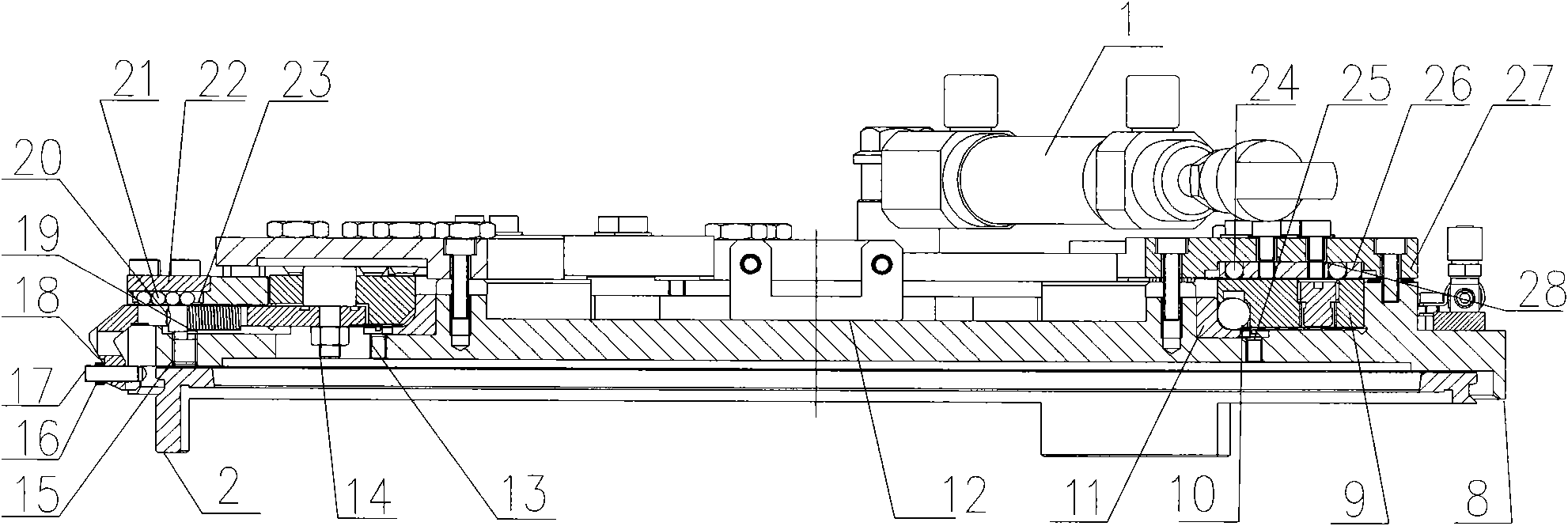
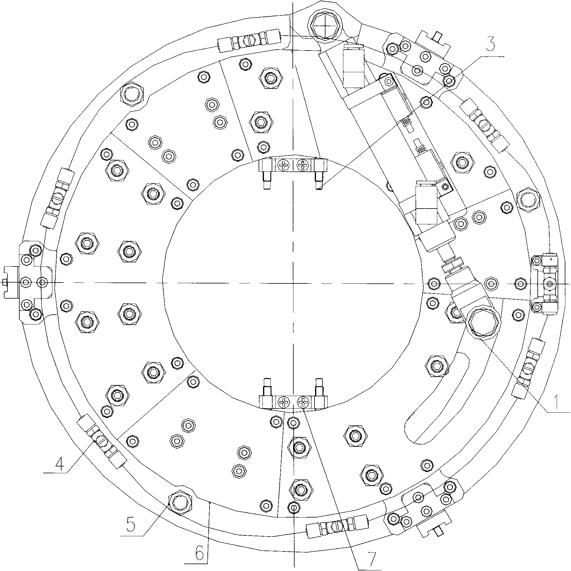
[0043] like figure 1 and figure 2 Shown is a silicon edge protector that includes:

[0044] fixed plate 8;

[0045] The triple eccentric cam disc 9 is mounted on the fixed disc 8, and the triple eccentric cam disc 9 has three evenly distributed eccentric grooves;

[0046] Cylinder mechanism 1, one end of which is installed on the fixed plate 8, and the other end is installed on the triple eccentric cam plate 9;

[0047] Three cam followers 14, which are respectively arranged in the three eccentric grooves of the three eccentric cam discs 9;

[0048] three protective claws 18, which are respectively mounted on the three cam followers 14 and embedded in the fixed plate 8;

[0049] The protection ring 2, which is installed directly under the fixed plate 8, and the protection claw 18 plays a role in fixing the fixed plate;

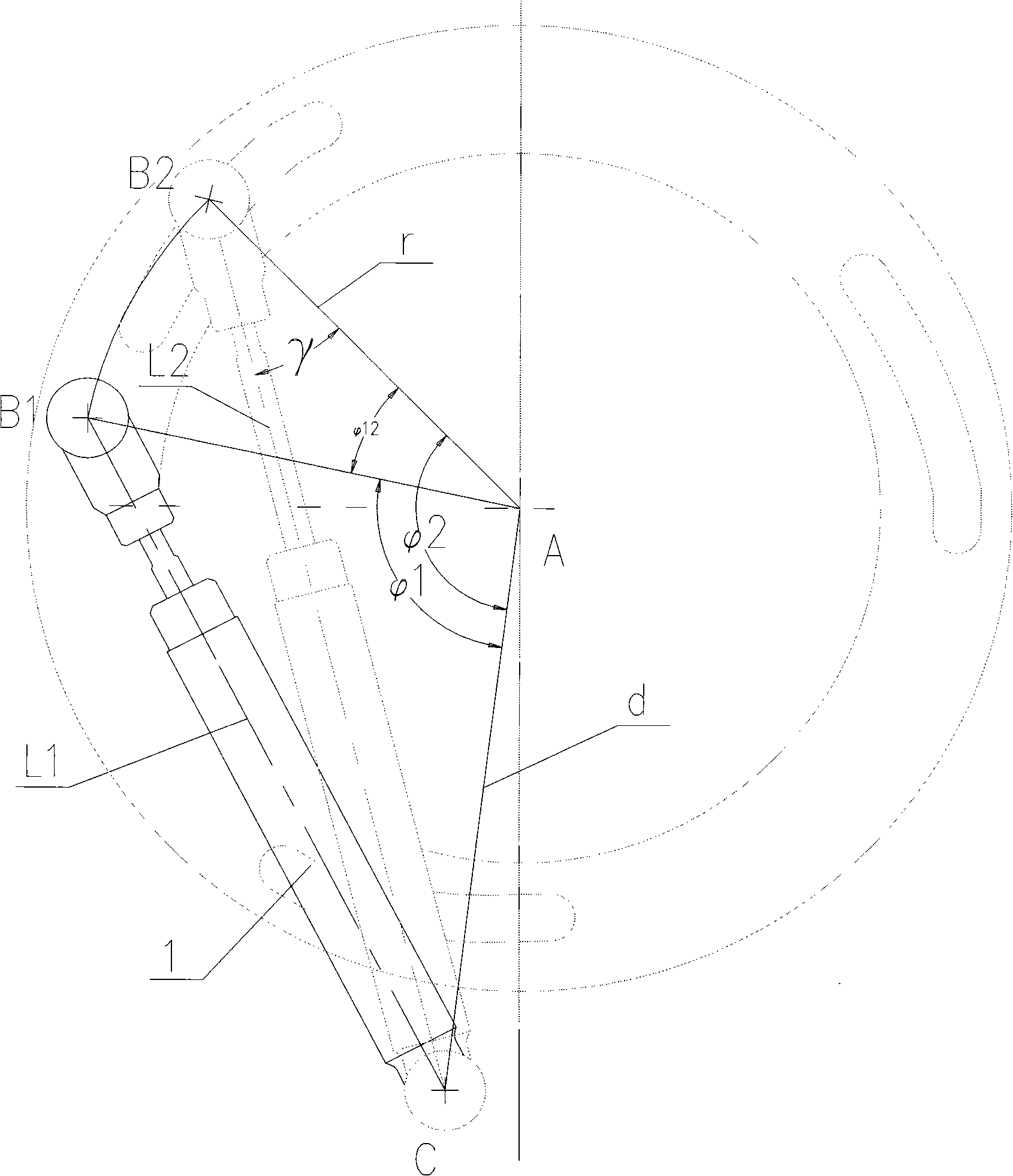
[0050] The silicon wafer edge p...


PUM


Abstract

The invention discloses a silicon chip edge protection device and an application method thereof. A cylinder, one end of which is arranged on a fixed disc and the other end of which is arranged on a three-eccentric cam disc, horizontally stretches and swings to drive the three-eccentric cam disc arranged on the fixed disc to perform circular motion; by a method of converting a linear motion into aplurality of equal synchronous radial motions in a vector conversion form, the linear swing is converted into the circular motion; the three-eccentric cam disc drives eccentric grooves on the cam disc to perform circular motion around respective circle center, so that a circular motion is converted a plurality of synchronous eccentric motions; the three-eccentric cam disc drives cams in the eccentric grooves to perform radial motion, so that the plurality of synchronous eccentric motions are converted into synchronous radial motions; and cam followers drive protection claws to perform radial motion, and the protection claws grip or lay down protection rings, so that exchange of the protection rings or other articles is realized. The device has high precision, good reliability, high repeated precision, simple structure, low need of power source and high synchronism.

Description

technical field [0001] The invention relates to the field of semiconductor manufacturing, in particular to a silicon wafer edge protection device and an application method thereof. Background technique [0002] Lithographic apparatuses are mainly used in the manufacture of integrated circuits IC or other micro devices. With a photolithographic apparatus, a mask pattern can be imaged on a photoresist-coated wafer, such as a semiconductor or LCD panel. The lithography device is exposed through a projection objective lens, and the designed mask pattern is transferred to the photoresist. As the core component of the lithography device, the edge protection device of the silicon wafer has the function of protecting the edge of the silicon wafer during the exposure process of the negative photoresist process. important influence. [0003] In order to obtain the imaging effect, a photoresist is coated on the silicon wafer, and a photosensitive material that can produce a corrosion...

Claims


Application Information

Patent Timeline
Patent Type & Authority Applications(China)
IPC IPC(8): G03F7/20
Inventor 吴荣基
Owner SHANGHAI MICRO ELECTRONICS EQUIP (GRP) CO LTD
Why Eureka
Try Eureka