Method and device for cleaning wafer

A technology for cleaning wafers and wafers, applied in cleaning methods and utensils, cleaning methods using liquids, chemical instruments and methods, etc., which can solve the problems of long residence time, different tangential speeds, and different degrees of removal

Inactive Publication Date: 2011-08-10
UNITED MICROELECTRONICS CORP
View PDF4 Cites 13 Cited by
  • Summary
  • Abstract
  • Description
  • Claims
  • Application Information

AI Technical Summary

Problems solved by technology

However, because during rotation, the tangential speeds of the regions with different distances from the center of the wafer on the wafer are different, thus causing different regions to be exposed to the rinse liquid at different times. For example, the tangential speed of the wafer edge is greater than that of the wafer center, so Rinse fluid at the edge of the wafer will be thrown off the wafer surface faster, while rinse fluid at the center of the wafer will stay longer
In this way, the residues on the surface of different positions of the wafer and the material layer on the surface are removed by the rinsing liquid to different degrees, resulting in poor uniformity of the wafer surface

Method used


Image

  • Method and device for cleaning wafer
  • Method and device for cleaning wafer
  • Method and device for cleaning wafer

Examples


Embodiment Construction

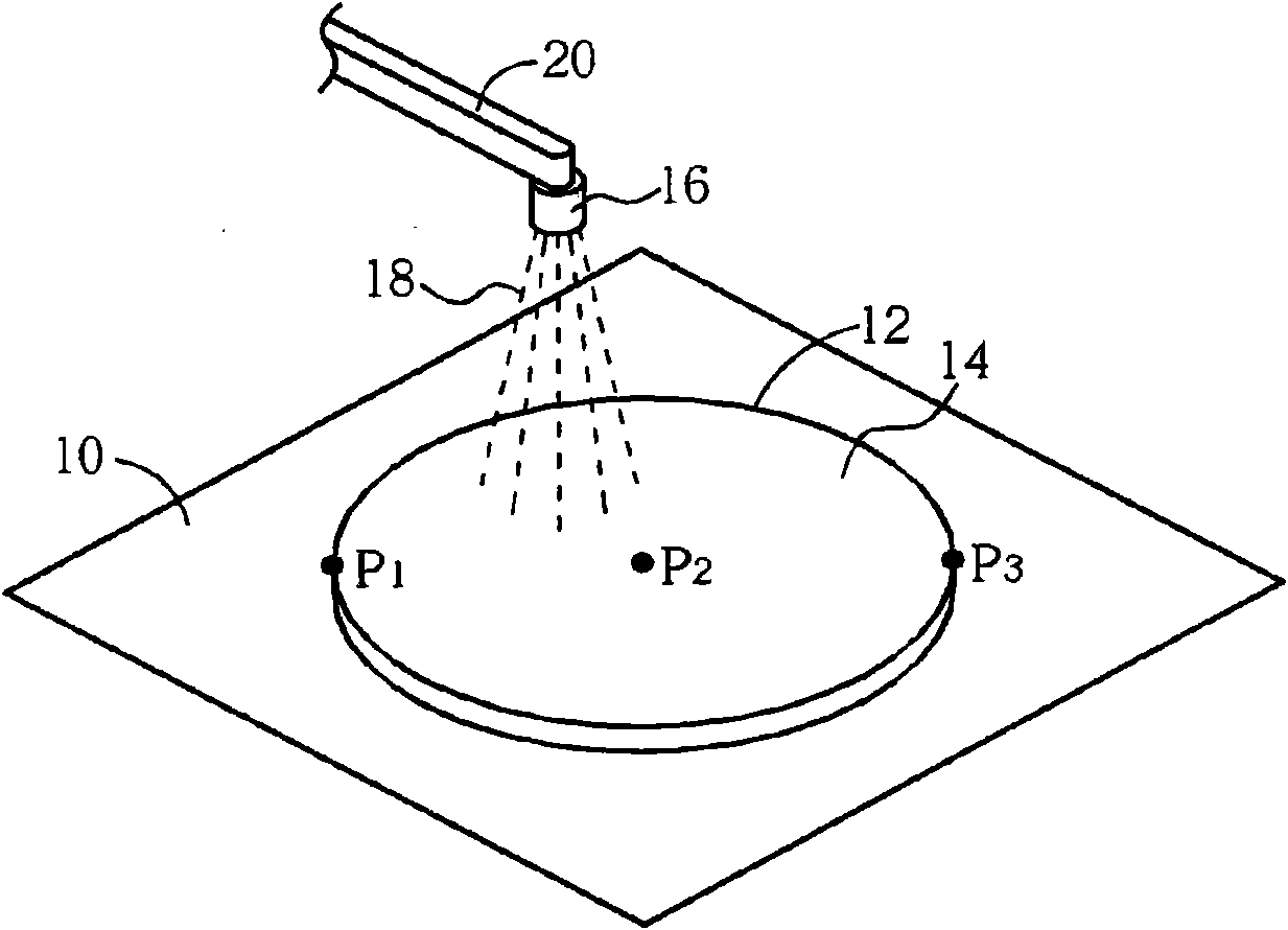
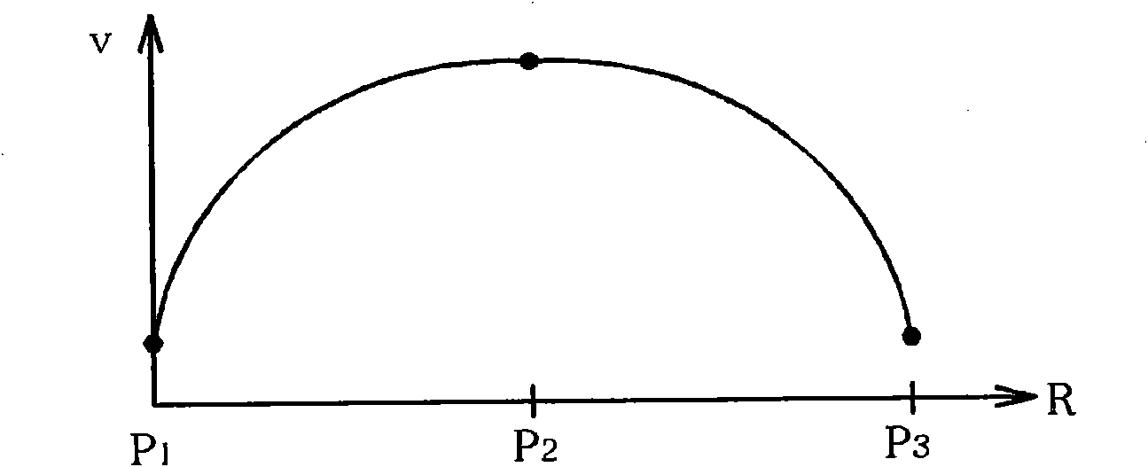
[0020] figure 1 The wafer cleaning method according to the first preferred embodiment of the present invention is shown. figure 2 A line graph showing the moving speed of the nozzle vs. the position of the nozzle according to the first preferred embodiment of the present invention. Such as figure 1 As shown, at first a platform 10 is provided for carrying and rotating a wafer 12, wherein the wafer 12 has a surface 14 to be cleaned, and a nozzle 16 is located above the wafer 12 for spraying a cleaning solution 18 on the surface 14 to be cleaned, The nozzle 16 is fixed to a control arm 20 which can be used to move the nozzle 16 horizontally. Carry out a cleaning step then, utilize platform 10 counterclockwise or clockwise with rotating speed 300~1000rpm, be preferably the rotating speed of 500rpm rotate wafer 12, and, utilize control arm 20 to move nozzle 16 at non-constant speed, by surface 14 to be cleaned A first given point P1 above moves to a second given point P2, the ...


PUM


Abstract

The invention discloses a method and a device for cleaning wafers. The method for cleaning wafers comprises the following steps: providing a platform for bearing and rotating a wafer, wherein the wafer is provided with a surface to be cleaned; arranging a nozzle above the wafer for spraying cleanout fluid on the surface to be cleaned; then cleaning: rotating the wafer; and moving the nozzle at non-constant velocity to a second set point from a first set point on the surface to be cleaned so that the time the first set point exposes to the cleanout fluid is same with the time the second set point exposes to the cleanout fluid. In addition, the nozzle moves slowly when close to the edge of the wafer, and moves faster when close to the centre of a circle of the wafer.

Description

technical field [0001] The invention relates to a wafer cleaning method, in particular to a cleaning method capable of maintaining the uniformity of the wafer surface. Background technique [0002] Semiconductor devices are fabricated from semiconductor wafers that undergo several processing operations. These operations include, for example, dopant implantation, gate oxide generation, interlayer dielectric layer formation, metallization deposition, line patterning, etching operations, chemical mechanical polishing (CMP), and the like. Usually after chemical mechanical grinding, etching, or photoresist development, there will be residues left on the wafer surface, such as chemical liquid components or chemical polymers. Therefore, in order to keep the wafer surface clean, it is necessary to properly clean the wafer. Give cleansing treatment. Usually, a liquid spraying device is used to use a rinsing liquid, such as a specific cleaning solution or deionized water, to remove ...

Claims


Application Information

Patent Timeline
Patent Type & Authority Applications(China)
IPC IPC(8): H01L21/00B08B3/02
Inventor 简金城吴俊元
Owner UNITED MICROELECTRONICS CORP
Why Eureka
Try Eureka