TFT-LCD (thin film transistor-liquid crystal display) array substrate and manufacturing method therefor

A technology of an array substrate and a manufacturing method, which is applied in the field of liquid crystal display, can solve problems such as TFT channel over-etching, and achieve the effects of reducing the number of processes, improving market competitiveness, and saving costs

Active Publication Date: 2011-08-10
BOE TECH GRP CO LTD +1
View PDF5 Cites 22 Cited by
  • Summary
  • Abstract
  • Description
  • Claims
  • Application Information

AI Technical Summary

Problems solved by technology

[0018] The invention provides a method for manufacturing a TFT-LCD array substrate, and also solves the problem of over-etching of TFT channels in the prior art

Method used


Image

  • TFT-LCD (thin film transistor-liquid crystal display) array substrate and manufacturing method therefor
  • TFT-LCD (thin film transistor-liquid crystal display) array substrate and manufacturing method therefor
  • TFT-LCD (thin film transistor-liquid crystal display) array substrate and manufacturing method therefor

Examples


Embodiment 1

[0105] image 3 It is a flow chart of Embodiment 1 of the manufacturing method of the TFT-LCD array substrate of the present invention. Such as image 3 Shown, the manufacturing method of TFT-LCD array substrate of the present invention comprises:

[0106] Step 1: sequentially depositing a first transparent conductive film, a first metal film and a doped semiconductor film on a transparent substrate, patterning a predetermined area to form a pattern including source electrodes, drain electrodes, data lines and pixel electrodes;

[0107] Step 2: Depositing a semiconductor thin film, patterning a predetermined area, and forming a pattern including a doped semiconductor layer, a TFT channel and a semiconductor layer;

[0108] Step 3: Depositing an insulating film and a second metal film, patterning a predetermined area, and forming a pattern including data line connection holes, gate lines, gate electrodes, and common electrode lines in the PAD area;

[0109] Step 4, depositin...

Embodiment 2

[0142] Figure 24 It is a flow chart of Embodiment 2 of the manufacturing method of the TFT-LCD array substrate of the present invention. Such as Figure 24 Shown, the manufacturing method of TFT-LCD array substrate of the present invention comprises:

[0143] Step 1: sequentially depositing a first transparent conductive film, a first metal film and a doped semiconductor film on a transparent substrate, patterning a predetermined area to form a pattern including source electrodes, drain electrodes, data lines and pixel electrodes;

[0144] Step 2: Depositing a semiconductor thin film, patterning a predetermined area, and forming a pattern including a doped semiconductor layer, a TFT channel and a semiconductor layer;

[0145] Step 3': Deposit an insulating film and a second metal film, pattern the predetermined area, then deposit a second transparent conductive film, perform a lift-off process and an etching process, and form data line connection holes, gate lines, and gate...

Embodiment 3

[0161] Figure 34 It is a flow chart of Embodiment 3 of the manufacturing method of the TFT-LCD array substrate of the present invention. Such as Figure 34 Shown, the manufacturing method of TFT-LCD array substrate of the present invention comprises:

[0162] Step 100: sequentially depositing a semiconductor thin film and a doped semiconductor thin film, or an insulating thin film, a semiconductor thin film and a doped semiconductor thin film on a transparent substrate, and patterning a predetermined area to form a pattern including a semiconductor layer;

[0163] Step 200: Depositing a first transparent conductive film and a first metal film, patterning a predetermined area to form a pattern including a source electrode, a drain electrode, a doped semiconductor layer, a TFT channel, a data line, and a pixel electrode;

[0164] Step 300: Depositing an insulating film, patterning a predetermined area, and forming a pattern including connection holes for data lines in the PAD...


PUM


Abstract

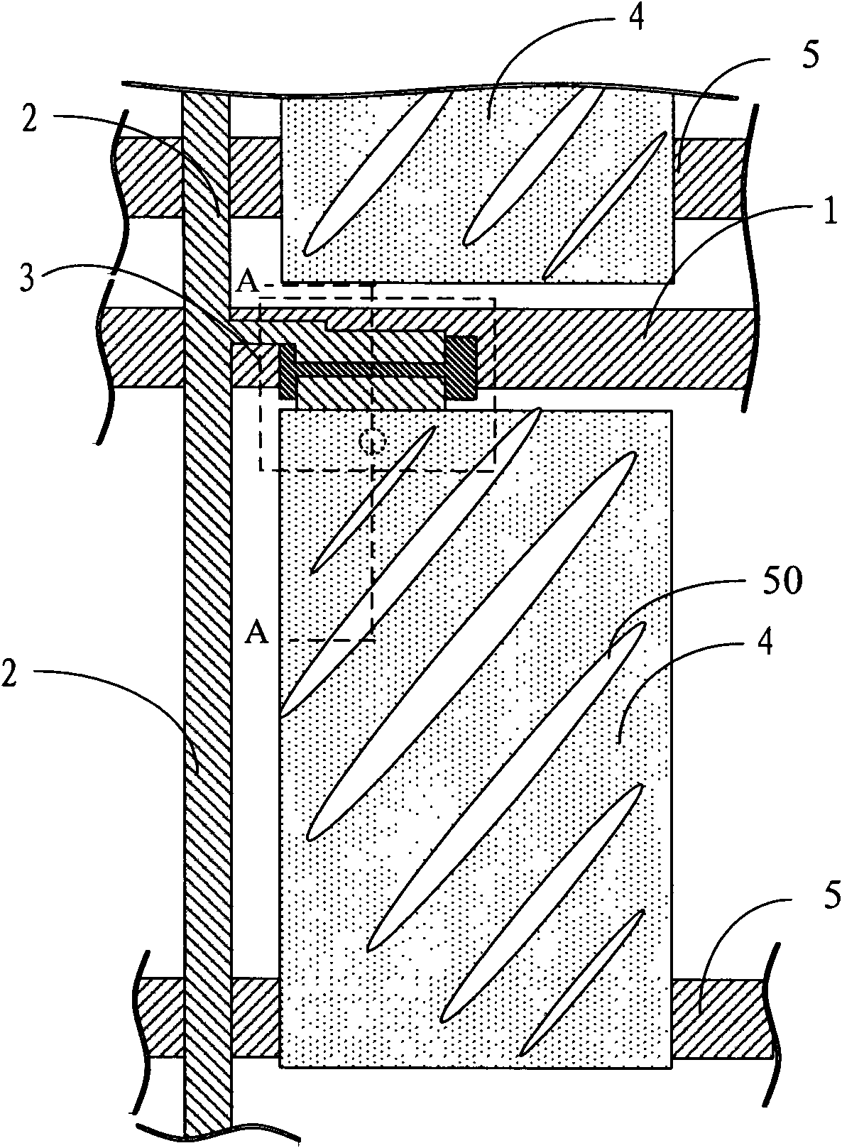
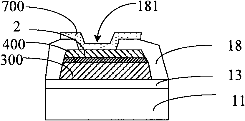
The invention discloses a manufacturing method for a TFT-LCD (thin film transistor-liquid crystal display) array substrate, which comprises the following steps: sequentially depositing a first transparent conductive film, a second metallic film and a doped semiconductor film on a transparent substrate and compositing a pattern for an established region so as to form the pattern comprising a source electrode, a drain electrode, a data line and a pixel electrode; depositing a semiconductor film and compositing a pattern for an established region so as to form the pattern comprising a doped semiconductor layer, a TFT (thin film transistor) channel and a semiconductor layer; depositing an insulating film and a second metallic film and compositing a pattern for an established region so as to form the pattern comprising a connecting hole of a PAD region data line, a grid line, a gate electrode and a public electrode line; and depositing a second transparent conductive film and compositing apattern for an established region so as to form the pattern comprising a public electrode. In the manufacturing method, the TFT-LCD array substrate is manufactured by a four-time pattern compositing process; and compared with the prior art, the manufacturing method reduces the process number, greatly saves the cost and improves the market competitiveness.

Description

technical field [0001] The invention relates to liquid crystal display technology, in particular to a TFT-LCD array substrate and a manufacturing method thereof. Background technique [0002] A Thin Film Transistor Liquid Crystal Display (TFT-LCD for short) is a main flat panel display (FPD for short). [0003] According to the direction of the electric field driving the liquid crystal, the TFT-LCD is divided into a vertical electric field type and a horizontal electric field type. Among them, the vertical electric field TFT-LCD needs to form the pixel electrodes on the array substrate and the common electrode on the color filter substrate; however, the horizontal electric field TFT-LCD needs to form the pixel electrodes and the common electrodes on the array substrate at the same time. Therefore, when manufacturing the array substrate of the horizontal electric field type TFT-LCD, it is necessary to add an additional masking process for forming the common electrode. Verti...

Claims


Application Information

Patent Timeline
Patent Type & Authority Applications(China)
IPC IPC(8): G02F1/1362G02F1/1368H01L27/12H01L21/336H01L21/77
CPCG02F1/13458G02F1/136227G02F2001/134372H01L27/1214H01L27/1288H01L27/124G02F1/136231G02F1/134372G02F1/1343G02F1/136286
Inventor 宋泳锡崔承镇刘圣烈
Owner BOE TECH GRP CO LTD
Why Eureka
Try Eureka