Interconnection structure for improving reliability of soldering spot of soft soldering of CCGA (Ceramic Column Grid Array) device and implementation method

An interconnection structure and reliability technology, which is applied in the manufacture of electric solid-state devices, semiconductor devices, semiconductor/solid-state devices, etc., can solve the problems of short service life and low reliability, and achieve improved and reliable resistance to mechanical external loads. The effect of improving the performance and reducing the degree of stress concentration

Inactive Publication Date: 2011-08-10
HARBIN UNIV OF SCI & TECH
View PDF3 Cites 18 Cited by
  • Summary
  • Abstract
  • Description
  • Claims
  • Application Information

AI Technical Summary

Problems solved by technology

[0006] The present invention solves the problem that the reliability of the existing area array packaging device is lower than that of ...

Method used


Image

  • Interconnection structure for improving reliability of soldering spot of soft soldering of CCGA (Ceramic Column Grid Array) device and implementation method
  • Interconnection structure for improving reliability of soldering spot of soft soldering of CCGA (Ceramic Column Grid Array) device and implementation method
  • Interconnection structure for improving reliability of soldering spot of soft soldering of CCGA (Ceramic Column Grid Array) device and implementation method

Examples


specific Embodiment approach 1

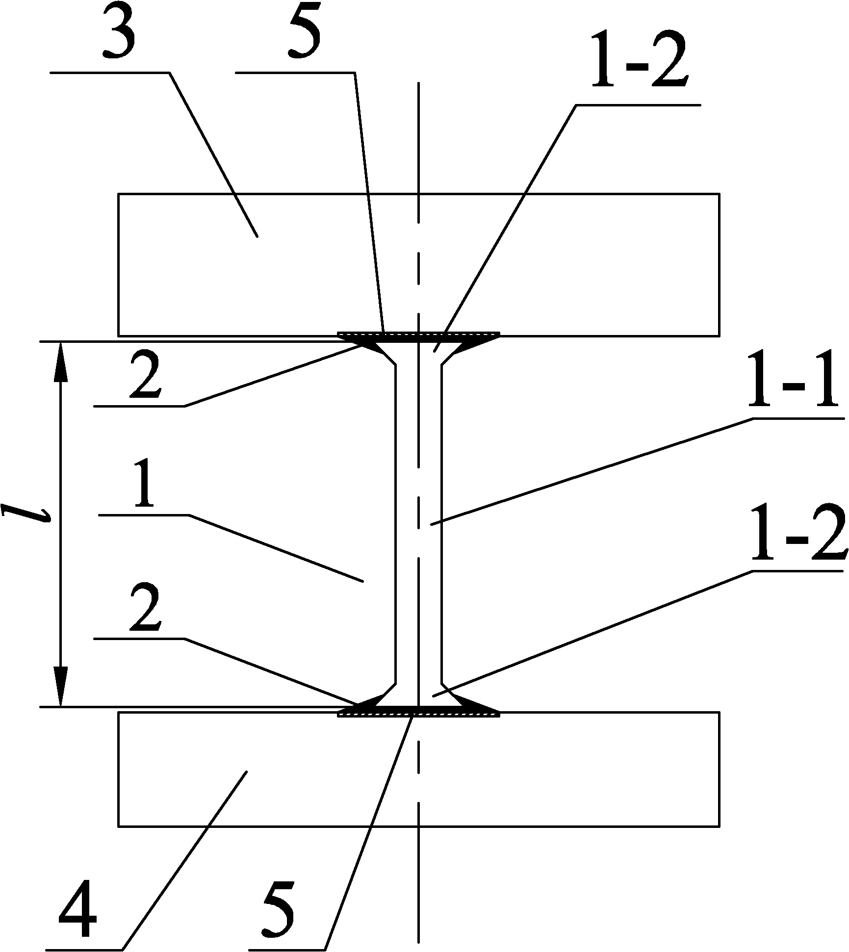
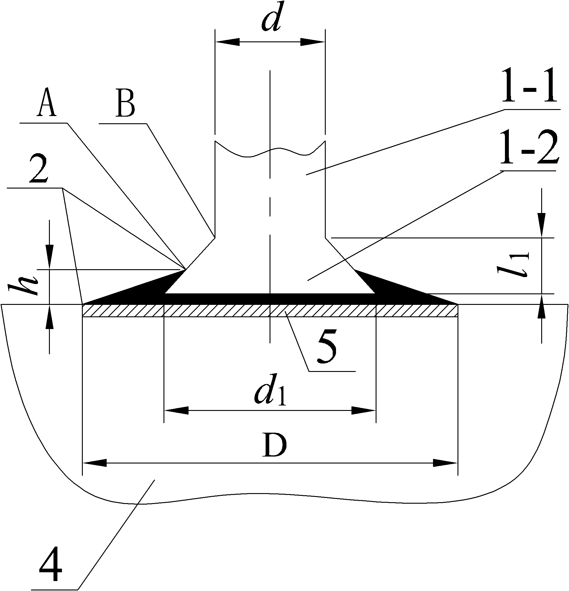
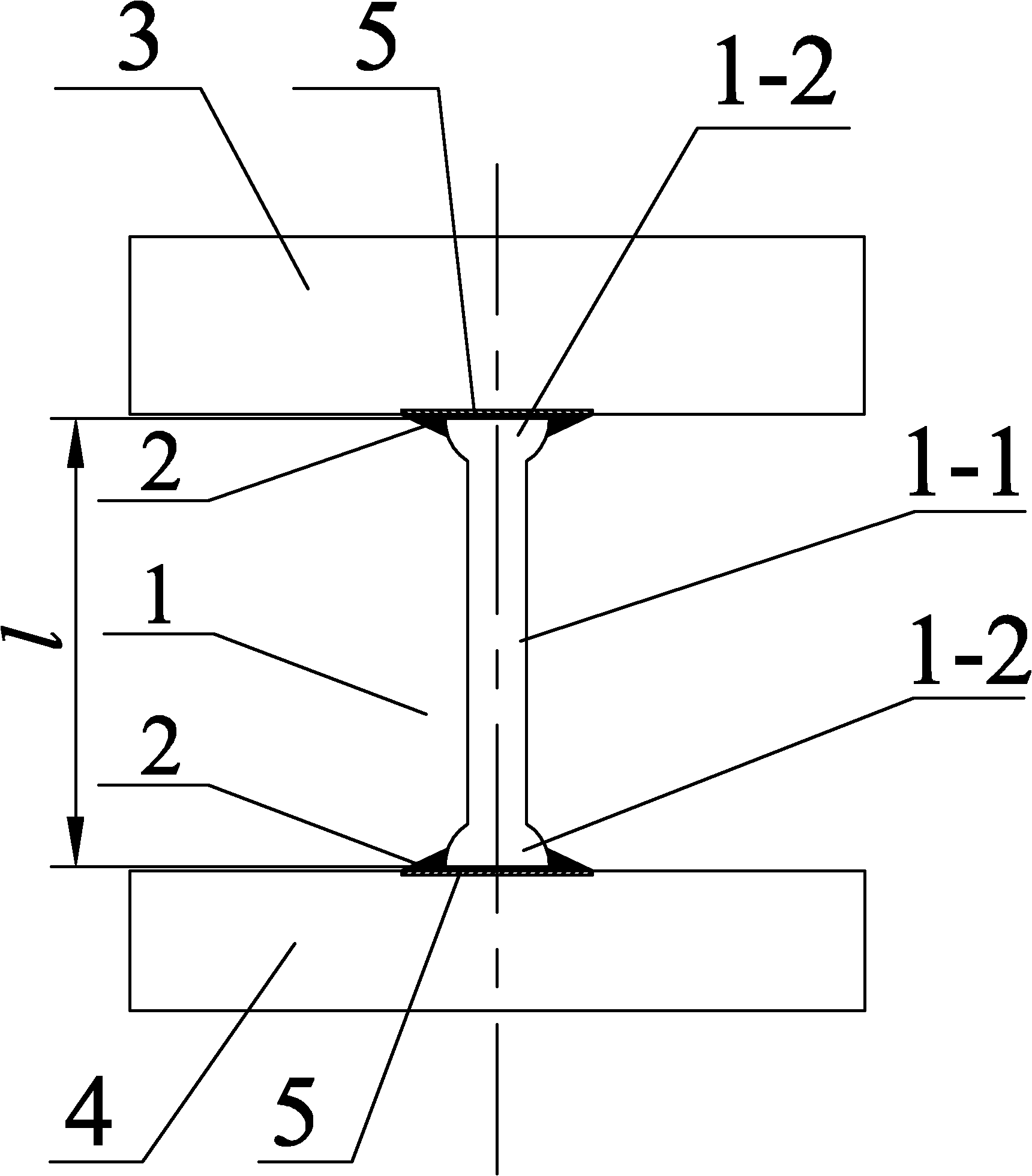
[0034] Specific implementation mode one: as Figure 1a , Figure 1b , Figure 2a , Figure 2b , Figure 3a and Figure 3b As shown, the interconnection structure for improving the reliability of soldering joints of CCGA devices described in this embodiment includes Cu pillars 1 and soldering fillets 2 located at both ends of Cu pillars 1, and the interconnection structure is used to realize chips or The mechanical and electrical connection between the metal film pads 5 on the chip carrier substrate 3 and the metal film pads 5 on the printed circuit board 4, the Cu column 1 is made of a cylinder 1-1 made in one piece and two ends The head 1-2 is formed, and each end 1-2 is in the shape of a rotary body with a straight line or an arc line as a generatrix. Coaxial, smooth transition between the cylinder 1-1 and the end 1-2; the height h of the brazing fillet 2 is less than the height l of the end 1-2 1 .

specific Embodiment approach 2

[0035] Specific implementation mode two: as Figure 1a and Figure 1b As shown, the shape of each end 1-2 in this embodiment is a truncated cone; the two ends of the cylinder 1-1 are respectively integrated with the upper bottom surface (small end face) of one end 1-2. Other components and connections are the same as those in the first embodiment.

specific Embodiment approach 3

[0036] Specific implementation mode three: as Figure 2a and Figure 2b As shown, the shape of each end 1-2 in the present embodiment is a ball table shape whose lower bottom surface radius is a ball radius (the ball table shape refers to the part where the sphere is cut by two parallel planes and clamped in the middle of the two planes); The two ends of the body 1-1 are made integral with the upper bottom surface (small end surface) of one end 1-2 respectively. Other components and connections are the same as those in the first embodiment.


PUM

PropertyMeasurementUnit
Diameteraaaaaaaaaa
Diameteraaaaaaaaaa

Abstract

The invention provides an interconnection structure for improving the reliability of a soldering spot of soft soldering of a CCGA (Ceramic Column Grid Array) device and an implementation method, belonging to the technical field of microelectronic packaging. The invention aims to solve the problems that the reliability of the conventional area array package device is generally lower than that of a peripheral leaded package device and a high-frequency and high-power large-area area array package device has low reliability and short service life. A Cu column in the interconnection structure consists of a cylinder and two end heads which are integrally formed; each end head is in the shape of a revolved body in which a straight line or cambered line is used as a bus; the cylinder is positioned between the two end heads which are arranged back to back, and the cylinder and the two end heads are coaxial; the cylinder is in smooth transition with the end heads; and the height of a soldering round corner is less than that of the end heads. The method comprises the following steps of: soldering one end of the Cu column on a metal film bonding pad at one side of a chip carrier substrate by using high-melting-point solder paste; and then soldering the other end of the Cu column on the metal film bonding pad at one side of a printed circuit board by using low-melting-point solder paste. The interconnection structure has high reliability and long service life and can be used for packaging a large chip.

Description

technical field [0001] The invention relates to an interconnection structure of a CCGA device and a realization method thereof, relates to the improvement of the internal interconnection structure of the CCGA device, and belongs to the technical field of microelectronic packaging. Background technique [0002] Lead-free, miniaturization, multi-function and high reliability are the direction of efforts in the manufacture of electronic products in recent years. Compared with the package form of four-sided pins, the number of input / output (I / O) per unit area in the package form of area array arrangement solder joints increases geometrically, which promotes the development of high-density packaging technology and makes electronic products Keep moving towards the goal of miniaturization and multi-function. However, the goal of high reliability has not been developed at the same time. The accelerated life test data show that compared with PBGA (Plastic Ball Grid Array) such a lea...

Claims


Application Information

Patent Timeline
IPC IPC(8): H01L23/52H01L21/60
CPCH01L2224/11
Inventor 赵智力孙凤莲
Owner HARBIN UNIV OF SCI & TECH
Why Eureka
Try Eureka